Engineering the Self-Assembly Pathway
Researchers engineer new pathways for self-assembled nanostructures
January 31, 2018
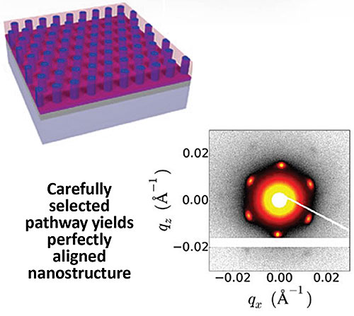
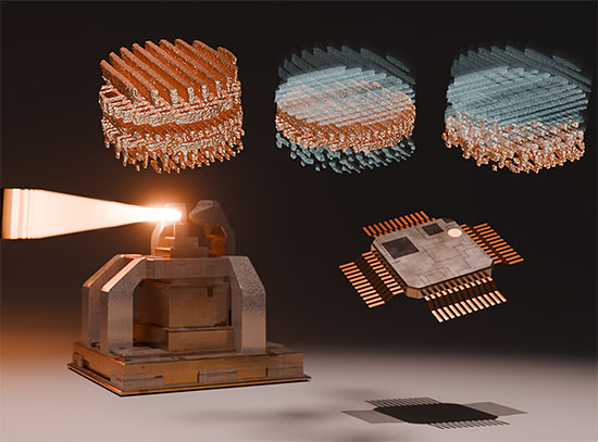
By selecting a multi-step process, scientists were able to grow a highly-ordered nanostructure through self-assembly (shown in red and blue). The yellow and red image shows the x-ray scattering data the scientists used to verify the order of the structure. Image credit: Nanoscale, 10, 416-427 (2018)
The Science
A new concept called “pathway-engineering” is described, where a sequence of processing steps is selected based on the ways a material can naturally order, thereby guiding the assembly towards a desired structure.
The Impact
By taking advantage of a material’s natural ordering, scientists can target previously unreachable structures for tailored functionality.
Summary
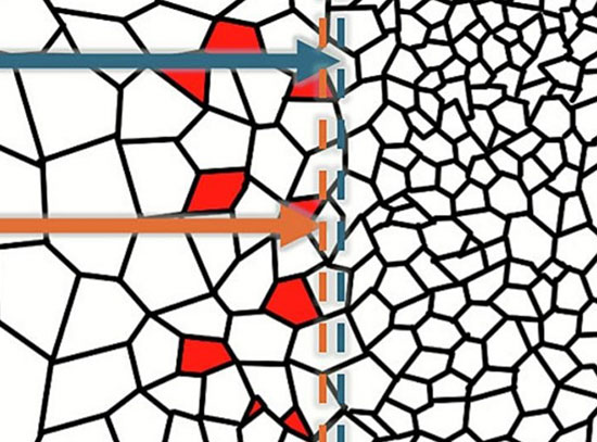
Self-assembly is a clever way to make nanostructures. Molecules are designed so that they spontaneously organize themselves into well-defined nanoscale objects that pack in a precise way. However, self-assembled materials frequently do not form the ‘optimal’ structure—that is, they may not form the structure desired by a scientist for a particular application. This often occurs because the system gets ‘stuck’ in the wrong structure and can’t rearrange into a different structure.
Therefore, scientists proposed and tested a new concept: “pathway-engineering.” In this concept, unlike in conventional material processing, where materials either get stuck in undesired configurations or must be strongly perturbed to enforce a desired structure, pathway-engineering takes advantage of the natural ordering behavior of materials, allowing new nanostructures to be formed in a simple and elegant way. This can be thought of as selecting a particular “pathway” in the landscape of all possible ordering histories.
In this work, scientists demonstrated how a block copolymer material that naturally forms nanoscale cylinders can be guided through the self-assembly process. By selecting a more complex sequence of processing steps (first shearing the material, then heating it), the self-assembling material can be coaxed into forming a well-aligned grid of nanoscale cylinders. The scientists used small-angle x-ray scattering (SAXS) at the Complex Materials Scattering (CSM) beamline to verify their results and to measure the exact order of the newly formed nanostructure. The CMS beamline is part of the advanced materials characterization suit available at the National Synchrotron Light Source II (NSLS-II), a U.S. Department of Energy (DOE) Office of Science User Facility located at DOE’s Brookhaven National Laboratory.
Overall, this new study provides a new way to create nanomaterials with desired functionalities.
Download the research summary slide
Related Links:
Feature Story: “Researchers Engineer New Pathways for Self-Assembled Nanostructures”
Contact
Chinedum O. Osuji
Yale University
chinedum.osuji@yale.edu
Kevin G. Yager
Brookhaven National Laboratory
kyager@bnl.gov
Publication
Y. Choo, P.W. Majewski, M. Fukuto, C.O. Osuji, K.G. Yager. Pathway-engineering for highly-aligned block copolymer arrays. Nanoscale, 10, 416-427 (2018). DOI: 10.1039/C7NR06069F
Funding
This research used resources of the Center for Functional Nanomaterials, and the National Synchrotron Light Source II, which are U.S. DOE Office of Science Facilities, at Brookhaven National Laboratory under Contract No. DE-SC0012704. C. O. and Y. C. acknowledge NSF support by DMR-1410568. P. W. M. acknowledges support of the Foundation for Polish Science, through the First Team program, co-financed by the EU under the European Regional Development Fund.
2018-17472 | INT/EXT | Newsroom