


Microelectronics
Brookhaven researchers are designing and characterizing electronic nanomaterials for next-generation microelectronic devices and architectures
Microelectronics are integral to the functioning of modern society and they play a central role in shaping the future. As demand grows for the use of microelectronics in advanced computing, artificial intelligence, sensing, communications, and other emerging technologies, new approaches are needed to improve performance, reduce energy consumption, enable new functionality, and accelerate the development of next-generation devices.
Brookhaven National Lab brings together collaborative, multidisciplinary scientific expertise and world-class facilities to address these challenges across the microelectronics innovation cycle: from the discovery and synthesis of new materials to device fabrication, advanced metrology, characterization under operating and extreme conditions, and codesign. Researchers are developing new materials, processes, measurement tools, and architectures, while providing the fundamental understanding needed to translate scientific discoveries toward scalable technologies.
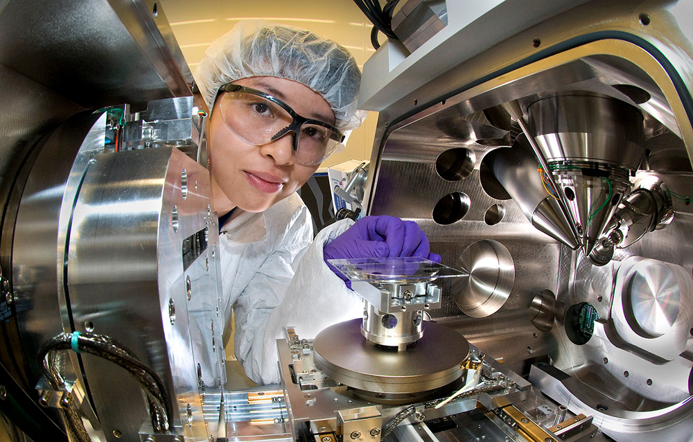
Center for Functional Nanomaterials
Brookhaven has expertise in the design, synthesis, patterning, integration, and characterization of electronic nanomaterials for next-generation microelectronic devices and architectures. Brookhaven’s Center for Functional Nanomaterials (CFN), a DOE Nanoscale Science Research Center, develops organic-inorganic hybrid materials for next-generation EUV lithography, 2D materials and heterostructures for future devices, atomic-layer processes for nanoscale manufacturing, and neuromorphic materials for beyond-CMOS computing. The Quantum Materials Press (QPress) supports controlled 2D-material transfer and integration.
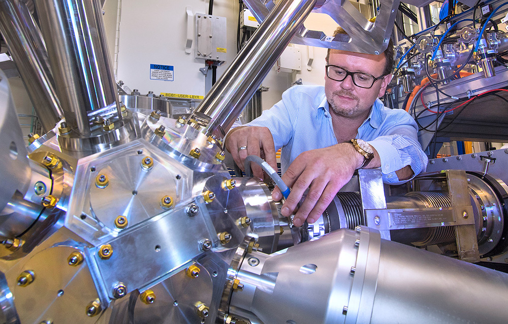
National Synchrotron Light Source II
The National Synchrotron Light Source II (NSLS-II), one of the most advanced synchrotron light sources in the world, boasts state-of-the-art x-ray scattering and microscopy beamlines and expertise in data analysis that can be used to visualize and probe microelectronic materials and devices under operating conditions. Scientists use these capabilities to understand and design next-generation semiconductor devices with improved performance, enhanced energy-efficiency, and new functionalities.
Advanced Metrology
Advanced metrology is essential to developing, fabricating, manufacturing, and packaging next-generation microelectronics. Brookhaven Lab is developing new synchrotron- and laboratory-based metrology tools for emerging materials and devices with increasingly complex structures and compositions. These tools enable non-destructive and in situ measurements of strain, defects, interfaces, failure mechanisms, dopant distributions, chemical composition, and electronic behavior, as well as nanoscale imaging, critical-dimension measurement, and electrical characterization. The resulting information links materials processing and structure to device performance and can inform future in-line manufacturing metrology tools.
Microelectronics Measurement
Brookhaven's National Synchrotron Light Source II (NSLS-II) is advancing a collaborative approach to addressing critical measurement challenges in microelectronics research and manufacturing. Through its Microelectronics Measurements Campaign Pilot, NSLS-II brings together researchers from industry, academia, and national user facilities to conduct coordinated experiments, develop advanced measurement and data-analysis methods, and accelerate the development of next-generation microelectronic materials and devices.
These collaborative campaigns leverage NSLS-II's advanced characterization capabilities and complementary expertise to address challenges in device fabrication, performance, reliability, and manufacturing.
Codesign
Brookhaven Lab’s codesign approach brings together materials discovery, device design, advanced characterization, modeling, and application requirements to accelerate the development of next-generation microelectronics. Through collaborations with industry and academia, Brookhaven applies co-design approaches that link materials synthesis, atomic-layer processing, nanoscale patterning, device fabrication, characterization, modeling, and system requirements. This iterative process enables materials and device measurements to guide design choices, while performance targets inform new materials and fabrication processes for future microelectronics.
Research Priorities
Energy-Efficient Microelectronics
The rapid growth of sensing, data processing, automation, and artificial intelligence requires microelectronics that operate with lower energy consumption. Brookhaven Lab researchers are developing new energy-efficient materials, devices, and architectures, including low-voltage, low-variability memristive devices and neuromorphic materials that may enable new approaches to information processing beyond conventional CMOS technologies.
Microelectronics for Extreme Environments
Microelectronics for space, nuclear systems, quantum technologies, and other demanding applications must operate reliably under conditions far beyond those encountered by conventional electronics. Brookhaven Lab has specialized capabilities for studying materials and devices under extreme conditions, including radiation exposure and deep cryogenic temperatures. Researchers use these capabilities to understand degradation and failure mechanisms and design devices with grater resilience, reliability, and operating lifetimes.
In particular, Brookhaven Lab’s Radiation Testing Facilities help reduce mission risk and enhance safety by supporting the development of more robust components like microelectronics, motion controls, power systems, and shielding.

The NASA Space Radiation Laboratory uses beams of heavy ions extracted from Brookhaven’s Booster accelerator to simulate cosmic rays found in space. Beams from protons to bismuth are accelerated up to 100-1500 MeV/u, with ion source changes as fast as 4 minutes. Uniform intensity beam sizes up to 20 x 20 cm2 enable large sample testing.

The Tandem Van de Graaff facility consists of two 14-megavolt electrostatic accelerators. It can provide ion beams for more than 50 ion species at a wide range of energies and intensities. Ions from 1 MeV protons to 337 MeV Gold can be provided. The Single Event Upset Test Facility is available for the study of space radiation effects, Single Event Effects Testing, and instrument calibration.
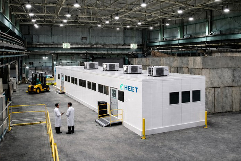
This proposed facility is being specifically designed to meet the growing national demand for high-energy heavy-ion testing. HEET will provide beam energies up to 2500 MeV/n, replicating over 75% of the cosmic ray spectrum, and will offer protons and ion species from helium to bismuth and above, plus advanced modes of supplying beam.
