Nanoconfinement of Organic Solar Cell Material Enhances Conductivity
Nanometer-scale restructuring doubles electricity output for the same amount of absorbed sunlight
October 24, 2011
Sometimes a change in surroundings makes all the difference. That’s the approach a group of researchers at the U.S. Department of Energy’s (DOE) Brookhaven National Laboratory has used to improve the electricity output of a semiconductor material used in polymer-based solar cells. By confining the light-absorbing/charge-separating material within nanometer-scale pores, instead of using it in continuous thin-film sheets, the scientists enhanced the material’s electrical conductivity by more than 500 times — and produced solar cells with twice the electricity output for the same amount of absorbed sunlight.
 enlarge
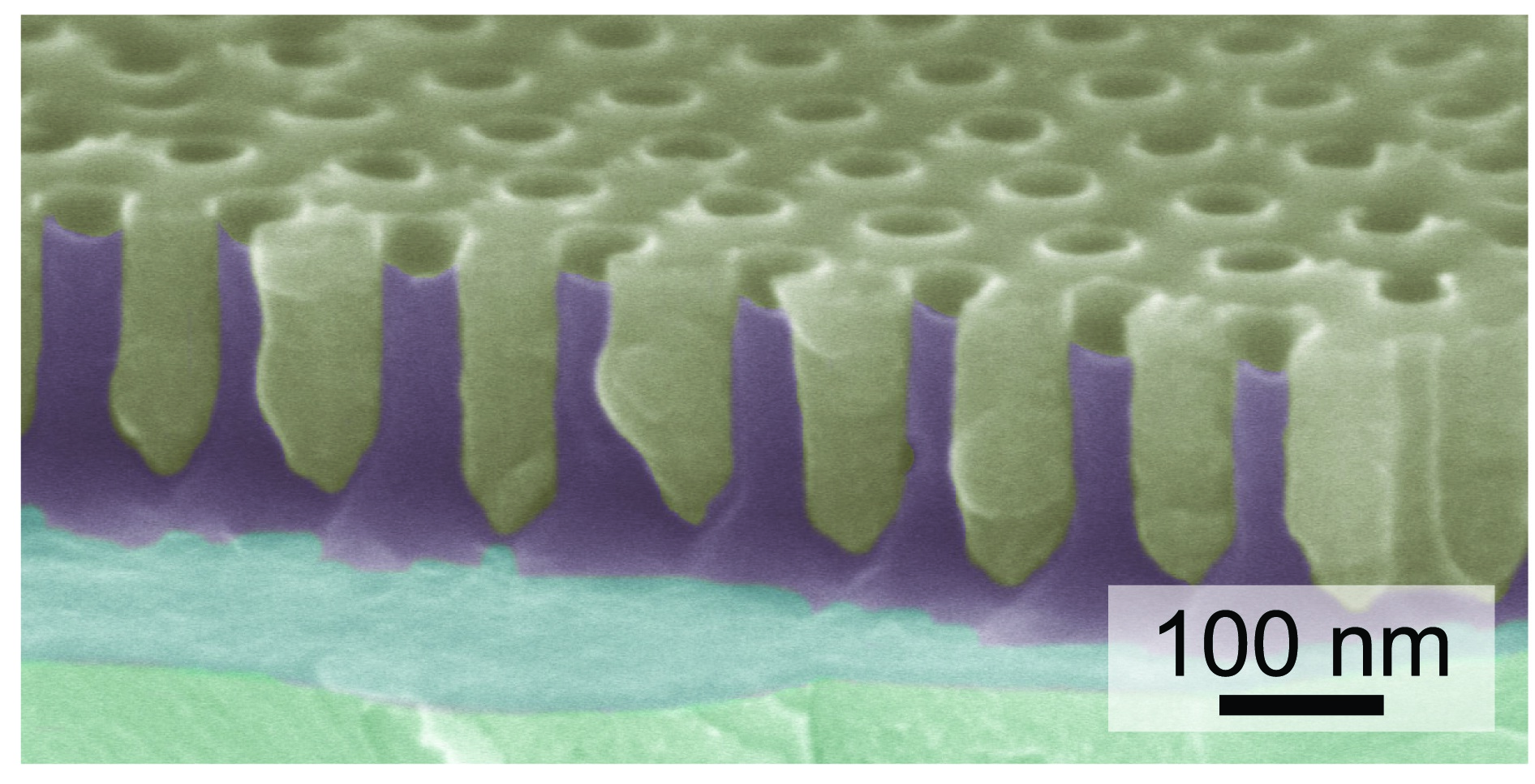
This angled view shows an aluminum oxide template (gray) with a regular array of 60-nanometer holes filled with an organic semiconductor (purple). This nanoconfined semiconducting polymer produces twice the amount of electricity for a given amount of absorbed sunlight as compared to the same material spread as a thin film.
The advance doesn’t improve overall solar-cell efficiency, however, because the nano-confined light-absorbing material doesn’t cover as much area as in the thin-film format. But the research suggests that such nanoscale restructuring, described in the cover article of the October 17, 2011, issue of Applied Physics Letters and in the September 13, 2011, issue of ACS Nano, might eventually achieve that goal, and make polymer-based solar cells — potentially manufactured as inexpensively as plastics — more competitive in the marketplace.
“Judged by their physical properties, organic semiconductors should be more efficient at converting sunlight to electricity than they are,” said Charles Black, group leader for electronic materials at Brookhaven’s Center for Functional Nanomaterials (CFN). “One of the goals of our research is to understand why — and to devise new solar cell architectures to improve them.”
The team, including materials scientist Jonathan Allen and other Brookhaven collaborators, focused its attention on a common blend of organic materials used in polymer-based solar devices. The blend is typically used as a thin film sheet between two conducting metal electrodes. Incident sunlight “excites” electrons in the organic semiconductor and produces electron-hole pairs. The blend helps separate these pairs and sends the electron to one electrode and the hole to the other in order to produce electricity.
“While the organic blend is very efficient at splitting electron-hole pairs, it’s not so good at transporting them out,” Allen said.
 enlarge
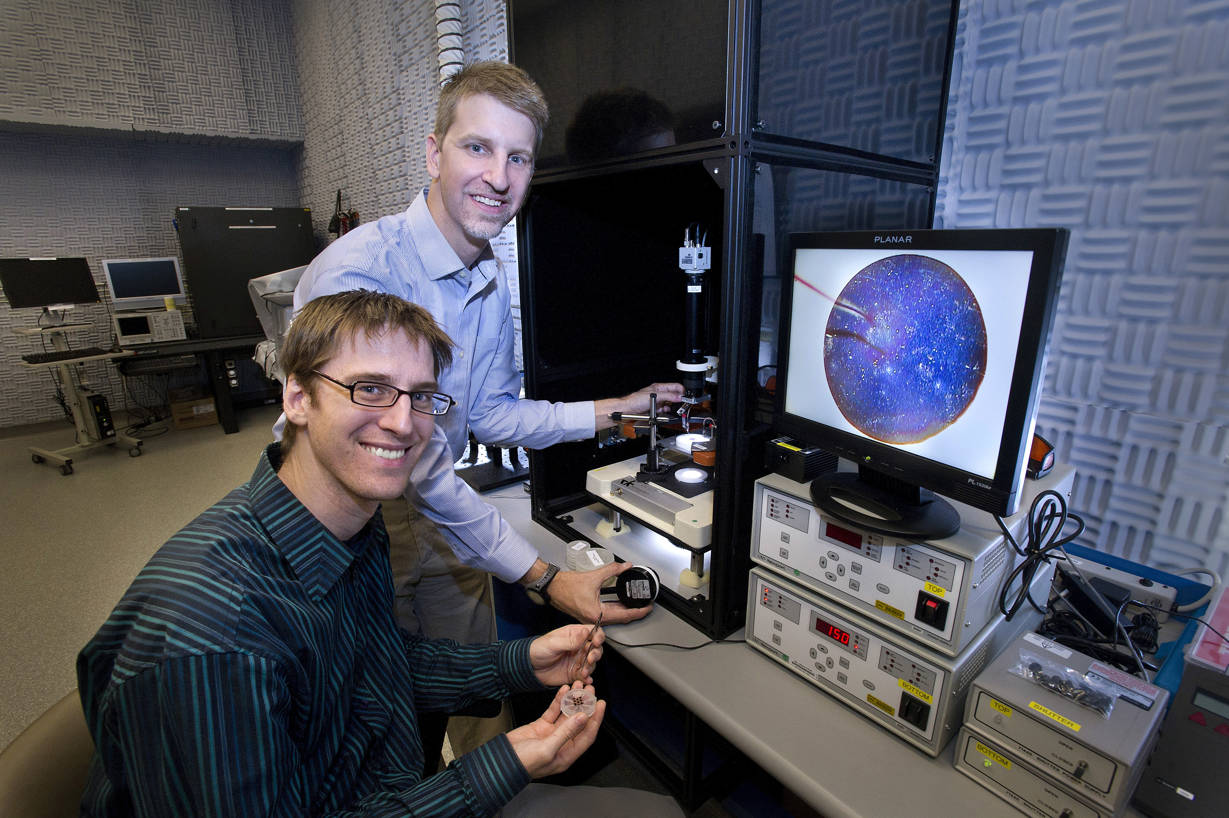
Charles Black (standing) and Kevin Yager, coauthors on this research, probing the properties of organic solar materials at the CFN.
To understand why, the scientists partnered with Kevin Yager (CFN) and Ben Ocko (Condensed Matter Physics Department) to examine the material using bright beams of x-rays at Brookhaven’s National Synchrotron Light Source (NSLS). By measuring the angles at which x-rays diffracted around molecules composing the organic film, the scientists determined that the molecules packed in such a way to enhance electrical conductivity in the plane of the film, but not perpendicular to it.
“Solar cells need electrons and holes to move in the out-of-plane direction — that is, toward the conductors designed to collect the current,” said Allen. “So we decided to try turning the material on its side by confining it to spaces more elongated in the out-of-plane direction.”
Back at the CFN, the scientists created a template of tiny holes measuring 60 nanometers in diameter and about 110 nanometers deep. Instead of generating each hole one by one, they used an electrochemical method to self-assemble arrays of billions of pores per square centimeter in a piece of aluminum foil.
“Flowing an electric current in an electrolyte will oxidize the aluminum in a particular way, creating regular arrays of nanometer-scale holes,” said Allen. “We can do this over large areas without the need for any specialized tools,” he added.
Then the scientists filled the holes with the polymer blend, added metal conductor layers on top and bottom, and measured the current produced while illuminating the device with artificial sunlight.
“The out-of-plane conductivity of the material confined to the holes is 500 times better than when it is formed as a thin film,” said Allen.
But the scientists were surprised upon measuring the crystal structure of the nanoconfined material at the NSLS. Instead of seeing crystals aligned in the out-of-plane direction — as if the material had been turned on its side — they saw no alignment to the crystal arrangement whatsoever.
“We didn’t expect such a highly conducting material to be randomly oriented, but it is,” said Ocko.
The team believes the orientation of crystal stacking in a thin film arrangement actively blocks the out-of-plane movement of electrical current. However, confining the same material within nanopores inhibits such long-range crystal alignment, thus removing the roadblocks to out-of-plane current flow.
Solar cells made from the reconfigured material produce twice as much electricity for the same amount of absorbed sunlight, compared to an unconfined, continuous film. While this is a substantial improvement in the material performance, the overall solar device efficiency remains unimproved because the confining nanostructured template occupies valuable space. And that space is not generating electricity.
The team is exploring ways to minimize that wasted space to better leverage the improved material performance. They also plan to investigate whether the nano-containment approach could provide similar benefits for other organic solar materials.
“We’re excited about the research directions these results suggest,” said Black. “They play to the strengths of the CFN, making great use of Brookhaven’s capabilities to correlate a material’s structure to its electrical function — and ultimately to improve its performance.”
This work was funded by the Department of Energy’s Office of Science and by Brookhaven’s Laboratory Directed Research and Development program.
The Center for Functional Nanomaterials at Brookhaven National Laboratory is one of the five DOE Nanoscale Science Research Centers (NSRCs), premier national user facilities for interdisciplinary research at the nanoscale. Together the NSRCs comprise a suite of complementary facilities that provide researchers with state-of-the-art capabilities to fabricate, process, characterize and model nanoscale materials, and constitute the largest infrastructure investment of the National Nanotechnology Initiative. The NSRCs are located at DOE’s Argonne, Brookhaven, Lawrence Berkeley, Oak Ridge and Sandia and Los Alamos national laboratories. For more information about the DOE NSRCs, please visit http://nano.energy.gov.
Visit Brookhaven Lab's electronic newsroom for links, news archives, graphics, and more or follow Brookhaven Lab on Twitter.
Scientific Papers
Enhanced Charge Collection in Confined Bulk Heterojunction Organic Solar Cells
2011-2563 | INT/EXT | Newsroom


