Nanoimprinting Controls Orientation of Organic Solar Polymers
Restructuring could lead to more efficient conversion of sunlight to electricity
September 12, 2011

Benjamin Ocko
As scientists attempt to improve the performance of organic photovoltaic devices — solar cells made from plastic-like polymers that absorb sunlight to produce electricity — they’ve discovered that how the molecules stack up can make a big difference. Finding ways to control molecular orientation is therefore a major goal of the emerging organic photovoltaic industry.
Now scientists at the U.S. Department of Energy’s Brookhaven National Laboratory have shown that “nanoimprinting” — stamping the polymer with a template etched with grooves measuring 50 billionths of a meter — imparts a sense of order among the polymer chains, orienting them in a preferred configuration that should improve solar-cell performance. The scientists describe their research on reorienting the polymers in an upcoming issue of ACS Nano, a journal of the American Chemical Society.*
“We can now control the alignment of the polymers using these very finely spaced grooved patterns to imprint features into the conducting polymers,” said Brookhaven physicist Benjamin Ocko, lead author on the paper. “The technique is analogous to imprinting designs into sealing wax with a stamp.”
Controlling the orientation of polymers is a much more complicated process, but it has led to important technological breakthroughs in a range of materials. Bulletproof vests, for instance, are made from the type of plastic used in grocery bags and milk jugs, yet by making the fibers well oriented and also crystalline, the material becomes much stronger. “Our imprinting approach to align polymers might lead to improved organic photovoltaic devices,” Ocko said.

Charles Black
“In organic solar cells, the electrical and optical properties of the polymer semiconducting materials are often not the same in all directions, because these properties are directly dependent on the molecular orientations of the polymer chains,” explained paper co-author Charles Black, leader of the Electronic Nanomaterials group at the Center for Functional Nanomaterials (CFN) at Brookhaven. “By optimizing the orientation and crystalline properties of these conducting polymers, we’re targeting significant improvements in solar-cell performance.”
The team has been exploring a variety of ways to make changes in the morphological arrangement of organic photovoltaic polymers to see how these changes affect their properties. In the present study, they worked with one of the most common and simplest of these polymers, poly-3(hexyl thiophene), or P3HT, which absorbs sunlight and helps conduct the light-generated current.
They made the thin films of P3HT at the CFN, then used a template etched with 50-nanometer-wide grooves spaced 100 nanometers apart to stamp the material while heating it to 150 degrees Celsius. The 50-nanometer grooves are ultra-narrow, corresponding to a distance of about 100 molecules. After removing the stamp, the scientists used high-intensity and focused x-rays at the Lab’s National Synchrotron Light Source (NSLS) to look at the material’s structure.
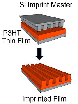
Aligning polymers: An imprint master is pressed into a P3HT thin film heated to 150 degrees Celsius. When the stamp is removed, the film remains imprinted with 100-nanometer-spaced grooves, as seen in the scanning electron micrograph. Supplemental x-ray scattering measurements show that this imprinting process aligns the polymers along the grooves and orients them in a configuration that should enhance the material’s performance in solar cells.
“We used a technique called x-ray diffraction, where we look at how the x-rays diffract, or bounce off, the surface, which allows us see the arrangement of the polymers,” said Htay Hlaing, a Stony Brook University graduate student who carried out the measurements.
The experiments showed that the grooves stayed imprinted into the material even after the stamp was removed, and even after the sample was reheated and cooled, which indicates that the arrangement is stable, Ocko said. The studies also revealed details of the material’s restructuring.
“We saw a very different diffraction pattern when the grooves were aligned with the direction of the x-ray beams compared with when they were perpendicular to the incoming beam,” said Kevin Yager, a scientist at the CFN who helped take measurements and analyze results. Previous studies could not pick up many of the details found in the present study since they lacked the resolving power provided by the high-intensity synchrotron beams and advanced detectors at the NSLS.
From the diffraction patterns of the scattered x-rays, the scientists were able to deduce that the polymer chains were well aligned along the grooves. Even more importantly, according to Black, “The imprinting reoriented the material in a way that we expect will improve the electrical properties between the top and bottom of the film, thus making the films better suited for photovoltaic applications.”
Polymers in an unstamped control sample, in contrast, were more randomly arranged, making them less suitable for photovoltaic applications.
Additional studies will test the effect of this new nanoimprinted material in conjunction with other solar cell components to see how the reorientation improves solar-cell efficiency.
“The specialized scientific tools we have at the CFN and NSLS allow us to tinker with basic properties and explore at a very fundamental level how we can strategically improve material performance,” said Ocko. “This ability to reorient polymers with nanoscale imprinting may eventually find applications in other fields, including molecular electronics.”
This research was funded by the DOE Office of Science and by the Energy Laboratory Research and Development Initiative at Brookhaven National Laboratory.
The Center for Functional Nanomaterials at Brookhaven National Laboratory is one of the five DOE Nanoscale Science Research Centers (NSRCs), premier national user facilities for interdisciplinary research at the nanoscale. Together the NSRCs comprise a suite of complementary facilities that provide researchers with state-of-the-art capabilities to fabricate, process, characterize and model nanoscale materials, and constitute the largest infrastructure investment of the National Nanotechnology Initiative. The NSRCs are located at DOE’s Argonne, Brookhaven, Lawrence Berkeley, Oak Ridge and Sandia and Los Alamos national laboratories. For more information about the DOE NSRCs, please visit http://nano.energy.gov.
Related Links:
* Scientific paper: Nanoimprint-Induced Molecular Orientation in Semiconducting Polymer Nanostructures
2011-2585 | INT/EXT | Newsroom


