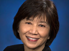
CFN Staff Spotlight: Esther Tsai Brings Expertise in X-ray Imaging
interview with a CFN staff member
August 27, 2019
 enlarge
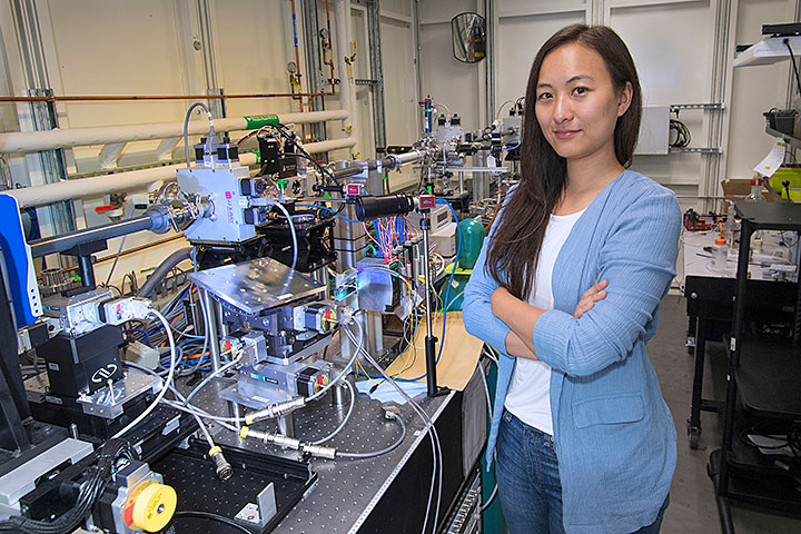
Esther Tsai at the Complex Materials Scattering beamline, operated in partnership between the Center for Functional Nanomaterials (CFN) and the National Synchrotron Light Source II (NSLS-II) at Brookhaven Lab.
The Center for Functional Nanomaterials (CFN) and the National Synchrotron Light Source II (NSLS-II)—both U.S. Department of Energy (DOE) Office of Science User Facilities at Brookhaven National Laboratory—have a strong research partnership. Staff members from the CFN have contributed to the development of new x-ray beamlines (experimental stations) for nanoscience, and they manage user programs at four beamlines. Key to the success of these programs is the expertise of CFN staff members, who help users with their experiments. Esther Tsai is one such staff member. She joined the CFN Electronic Nanomaterials Group in September 2018, bringing her experience in providing user support at the Swiss Light Source (SLS) at the Paul Scherrer Institute (PSI), where she completed postdoctoral research in x-ray ptychographic tomography. She holds a PhD and BS in electrical engineering from Purdue University with a focus on computational imaging and data analysis.
What is x-ray ptychographic tomography?
It is a technique for the high-resolution imaging of 3-D structures in large sample volumes. A resolution of tens of nanometers can be attained for a 100-micron (0.1 millimeter) sample volume. To perform the technique, you scan a small focused x-ray beam (about 10 microns, or 0.01 millimeters) over a sample as the sample is rotated in small increments. With every illumination, the beam gets scattered by the sample to produce a diffraction pattern that is collected by a detector. The patterns from overlapping illuminated regions are fed into a numerical reconstruction algorithm to reconstruct a 3-D image of the sample.
 enlarge
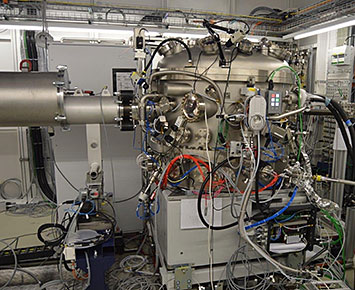
The 2-D ptychography system at the Swiss Light Source Coherent Small-Angle X-ray Scattering beamline. Credit: PSI.
In general, x-ray ptychographic tomography has two steps. The first step is ptychography—scanning a sample with the x-ray beam in two dimensions and recording the diffraction pattern at each position. The second part is tomography, which is based on the same idea as the CT (computed tomography) scans you get at the doctor’s office. A tomogram is 3-D visualization of the sample.
Ptychography has become more popular recently because of advances in hardware, and also because the algorithms and computational power are catching up. Scanning generates a lot of data, which need to be processed. The algorithms have been optimized to run on central and graphics processing units (CPUs and GPUs) in real time, as the experiments are being done.
At SLS, you conducted your own research in x-ray ptychographic tomography and provided user support. Can you explain this dual role?
I was at SLS for three years. A third of my time was spent helping users of the Coherent Small-Angle X-ray Scattering (cSAXS) beamline, which is dedicated to two imaging techniques: SAXS and ptychography. My support focused on ptychography.
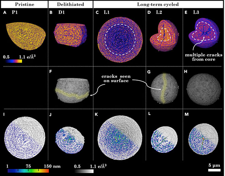
The rest of my time was dedicated to my personal research, which was split into two parts. The first was a battery project conducted in collaboration with an electrochemistry group at PSI. We were studying a lithium-ion battery material made of nickel, manganese, and cobalt to see if its internal structure changed from its original state after it underwent short- and long-term cycling (up to 100 charge and discharge cycles). We observed the 3-D formation of cracks in some of the battery particles and wanted to know how these particles crack. We discovered that the chemical composition of the particles was quite different from what the electrochemists had expected to see. The sphere-shaped particles had a surprising core-shell structure in which the middle of the particles looked different compared to the outside.
 enlarge
Ptychographic x-ray computed tomography for lithium-rich battery particles made of nickel, manganese, and cobalt in their pristine (i.e., original) (A), delithiated (i.e., removal of lithium) (B), and cycled (C–E) states. Cracks originating from the particle cores can be seen in (B), (D), and (E). The exterior of cracked particles is shown in (F–H), and surface cracks appear on particles in (F) and (G) while particles in (H) remain intact. As revealed in the particle cross-sections, the pristine particles (I) have smaller pores (dark blue) than the delithiated (J) and cycled (K–M) particles. The linear color scale corresponds to the electron density. Source: Cell Press, vol. 11, Jan. 2019, pgs. 356–365.
For the other half of my research, I focused on algorithm development. In particular, I was trying to optimize an algorithm to increase the image resolution of ptychography. Inherently, the image resolution is limited by the sample thickness. As the thickness increases even slightly, the resolution becomes degraded. Thickness is important because many samples are not homogenous, meaning they have different features throughout. If you only look at a thin slice of your sample, you may not get a representation of the larger volume. For example, when we study healthy versus diseased samples, the indicators of disease might only be in certain regions, and a small sample might miss these regions of interest. The problem is that when the sample becomes too thick, the current algorithmic model gives bad resolution and no longer provides an accurate description of the physics. In my research, I was trying to incorporate real physics into the model for thick samples while maintaining the resolution by using multi-slice ptychography, in which a thick sample is virtually sliced up into a set of thin slices.
What are some examples of the types of samples that scientists imaged with x-ray ptychographic tomography at the cSAXS beamline? Are there any that particularly intrigued you?
There was such a variety of samples, including mouse and human brains, fuel cells, lithium-ion batteries, fossils, mantis shrimp and other sea creatures, meteorites, and historical statues.
 enlarge
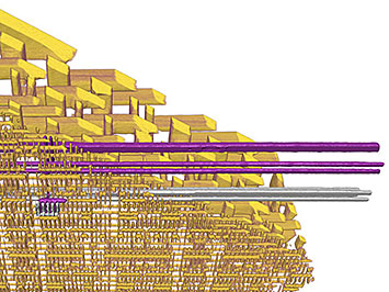
Using x-ray ptychographic tomography at the Swiss Light Source, scientists reconstructed a 3-D image of the nanosized transistors and wiring (yellow) inside an Intel microchip. Several interconnections linking the transistors have been colored. Credit: Paul Scherrer Institute/Mirko Holler.
One of the cool samples was a computer chip. The users imaged its internal structure (reported in Nature). The ability to look inside a chip and see the various circuit components—for example, copper electrical wires and silicon transistors—is important to both industry and the government. From an industry perspective, chip inspection can be used to perform quality control checks during the manufacturing process to ensure the structure is built according to the specifications. On the government side, it can be used to verify that a chip has only the features it should have, and not any other hardware that could be used for malicious activities, such as espionage.
How has your past experience prepared you for your current position at the CFN?
My time at SLS introduced me to the synchrotron community and various x-ray techniques. Moreover, the beamline users I interacted with were very diverse, both in where they came from—mostly from countries all over Europe and some from the United States—and their scientific backgrounds and mindsets. I had the opportunity to work with geologists, materials scientists, biologists, and many other kinds of scientists. I also had the opportunity to be a short-term summer visitor at the National Synchrotron Radiation Research Center in Taiwan.
Growing up in Taiwan and then living in the United States for school and in Europe for my postdoc exposed me to many different cultures. I think that exposure has trained me well to interact with a diverse user community.
Which CFN/NSLS-II partner beamlines are you providing user support for?
I provide user support for two x-ray scattering beamlines: Complex Materials Scattering (CMS) and Soft Matter Interfaces (SMI). At CMS and SMI, users can perform SAXS and wide-angle x-ray scattering (SAXS/WAXS) measurements. Both SAXS and WAXS record how x-rays are scattered after interacting with a sample, providing structural information about materials on a nanoscopic or angstrom scale.
You mentioned that you focused on x-ray ptychographic tomography at SLS. Now you are focused on SAXS and WAXS. What has that transition been like?
I’m bringing my knowledge and research experience. I’ve also been learning a lot from the beamline scientists, who have been so supportive, especially Ruipeng Li (CMS) and Guillaume Freychet (SMI). A very cool thing about measurements for SAXS/WAXS is that they are much faster than those for tomography experiments, and this speed makes studying in situ dynamics possible.
We have a lot of users, and they bring in different research topics and sample types. It’s very interesting to learn from them about these various materials and their applications while offering my experience in imaging and data analysis to advance our collaborative research.
Besides providing user support, what else are you working on currently?
I’m collaborating with Xiaohui Qu, a staff scientist in the CFN Theory and Computation Group, to set up a web-based interface for a software called Jupyter that will allow CFN users to access and analyze their beamline data remotely from their home institution.
I’m also in the early stages of a Department of Defense–funded project with Samuel Tenney, a chemist in the CFN Interface Science and Catalysis Group. We will use scanning electron microscopes and transmission electron microscopes at the CFN in conjunction with the CMS and SMI beamlines at NSLS-II to study the phase changes of energetic materials (i.e., explosives). Right now, we’re in the process of hiring additional team members, including a postdoc.
I’m also working with my CFN group leader Kevin Yager and Sungsoo Ha of Brookhaven Lab’s Computational Science Initiative (CSI) on improving and deploying a software for visualizing beamline datasets in real time.
Another effort I am involved in is developing machine learning (ML) algorithms for ptychography in collaboration with NSLS-II Hard X-ray Nanoprobe (HXN) beamline scientist Xiaojing Huang and PhD student Ziqiao Guan from Stony Brook University. At HXN, it currently takes a day or two to acquire ptychography images for 3-D samples. Our thought is that maybe ML can assist the conventionally used algorithm to increase the imaging speed while maintaining high resolution. High-throughput (and thus more statistics) is one advantage of faster measurements. Another advantage is that it will be possible to capture fast in situ dynamics, such as how a material’s structure changes as it is heated or cooled. Faster measurements also mean that samples are exposed to the x-ray beam for less time. Minimizing the exposure time is important for biological samples and other soft materials, which are very sensitive to x-rays and can deform in response to high x-ray doses.
 enlarge
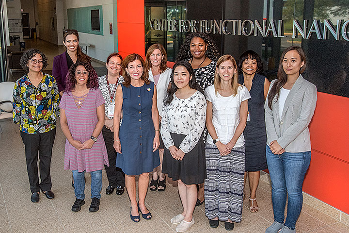
On August 20, 2019, Esther Tsai (far right) and other women from Brookhaven Lab participated in a roundtable discussion with New York Lt. Governor Kathy Hochul (second from left, front row) about diversity in science, technology, engineering, and mathematics (STEM). Tsai believes in doing outreach to encourage everyone, especially women and minorities, to pursue STEM without feeling intimidated. Front row (from left): DOE Brookhaven Site Office Contracting Officer Kim Nekulak, New York Lt. Governor Kathy Hochul, CFN Research Associate Christine Wang, NSLS-II Manager Lisa Miller, and CFN Staff Scientist Esther Tsai. Back row (from left): Office of Educational Programs Administrator Aleida Perez, CFN Assistant Director Priscilla Antunez, Special Assistant to the Director of External Affairs and Stakeholder Relations Office Janice Epstein, Environmental and Climate Sciences Department Chair Allison McComiskey, Collider-Accelerator Department Research Associate Jasmine Hatcher, and Inclusion and Diversity Manager Shirley Kendall.
You have a unique background that combines experience in user support, synchrotron x-ray imaging techniques, and computational data processing and analysis. How do you think your expertise can bring new perspectives to the CFN?
My experience working with physicists, chemists, and materials scientists, as well as my personal research in algorithm development could help form additional partnerships between the CFN/NSLS-II and CSI. I think there are great opportunities for collaboration. For example, visualization and ML tools could greatly help us analyze data more quickly to extract key features for making strategic decisions in real time during limited experiment time at beamlines.
If you would like to become a CFN user of the CFN-NSLS-II partner beamlines, you are encouraged to submit a research proposal through the CFN User Proposal System. For more information, contact the CFN User Office.
Brookhaven National Laboratory is supported by the Office of Science of the U.S. Department of Energy. The Office of Science is the single largest supporter of basic research in the physical sciences in the United States, and is working to address some of the most pressing challenges of our time. For more information, please visit science.energy.gov.
Follow @BrookhavenLab on Twitter or find us on Facebook.
2019-16756 | INT/EXT | Newsroom


