CFN User Spotlight: Frances Ross Studies Nanowire Growth
interview with a CFN user
April 21, 2016
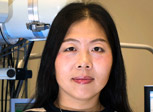
Frances Ross
Frances Ross, a materials scientist at IBM’s Thomas J. Watson Research Center in Yorktown Heights, New York, studies the mechanism by which atoms spontaneously self-assemble into nanowires—structures that are thousands of times longer than they are wide. Understanding how nanowires spontaneously form under different conditions requires instruments capable of capturing, at high resolution, the atomic-layer growth process as it occurs. Inside an environmental transmission electron microscope at the Center for Functional Nanomaterials (CFN), a Department of Energy Office of Science User Facility, filming is underway.
How did you come to study nanowires, and why do they interest you?
I enjoy both art and science and feel a close connection between the two, so I was attracted to electron microscopy from an early age. It is fascinating to me to use images and movies from an electron microscope to understand the ways that atoms arrange themselves into crystals or create new structures. Over the last few years, I have become interested in the growth of nanowires, crystals that are very long (micrometers) but narrow (10s of nanometers in diameter) and are made of different semiconducting materials.
Nanowires are interesting from several different perspectives. The process by which nanowires grow teaches us a lot of basic physics about crystal growth in general, as well as about catalysis, self-assembly, and nanostructure behavior. This information helps us tune the growth conditions to create nanowire-based structures with particular functionalities. The long, narrow geometry of nanowires and the sequential way they grow—one layer of atoms at a time is added to the end of the nanowire—allow fabrication of complex structures. For example, a nanowire made of one semiconductor can contain even smaller regions of a different semiconductor that have particular electronic properties. Nanowires have been used to build electronic devices such as low-power transistors, sensors, battery anodes, and solid-state lighting, with properties that can be optimized for each application.
What is required for a nanowire to grow in an electron microscope?
All the nanowires we study grow from small catalytic particles. The nanowires we study at CFN are made of silicon. To grow these silicon nanowires, we put catalysts—typically tiny crystals of a metal such as gold—onto a flat substrate that is loaded into the microscope. Then, we heat the substrate (to say 500 degrees Celsius) and flow a gas that contains silicon (we use a gas called disilane). The gas reacts with each metal particle, depositing silicon beneath the particles to build up the nanowire one layer of atoms at a time. Conveniently for us, because of their nanoscale dimensions, nanowires can be imaged directly in any transmission electron microscope (the electrons can pass through the diameter of the nanowire). We can, therefore, record images showing the nanowires’ shape, size, and atomic-level structure. But, even better, if the microscope has the capability to record images at the same time that we heat a sample and flow reactive gases—a capability of environmental transmission electron microscopes—we can make a movie of the nanowires as they grow.
 enlarge
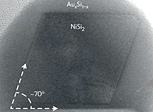
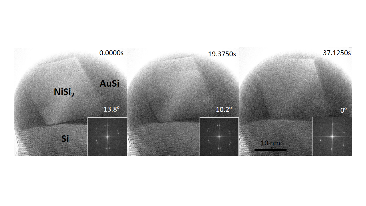
This series of images recorded at the CFN's environmental transmission electron microscope shows part of the process by which a nanoparticle is incorporated within a silicon nanowire. The first step (not shown) is to form an octahedral NiS2 nanocrystal within the catalyst droplet (AuSi) at the tip of the Si nanowire. The next step is for the nanocrystal to touch the Si nanowire (first image) and then rotate (second image) until the silicide and silicon crystals are in perfect alignment (third image). The insets show how the angle between the two crystal structures is measured from the Fourier transform of each image. The movie was recorded at 500°C at a rate of 400 images per second.
Which nanowire materials and growth conditions have you tested so far, and which are you interested in exploring?
We have grown silicon, germanium, gallium arsenide, and gallium phosphide nanowires at many different temperatures and gas pressures and with various types of catalysts in our lab, but at CFN we have focused on silicon nanowires. We have grown nanowires with junctions between materials—you first flow one gas to grow one material and then flow another gas to grow the next material on top. We have also made nanowires that contain smaller nanocrystals within them and looked at ways to control the arrangement of the atoms within each nanowire.
The types of materials and growth conditions we test are dictated by the possibilities of real-world applications, but they all show us glimpses of the underlying physics involved. Our current interest is in growing nanowires that form bridges between two electrical contact pads. For developing nanowire applications, it is essential to relate the electrical performance of a single nanowire to its physical structure, especially the structure at the two ends where the nanowire meets the “macroscale” world.
Have any of your findings surprised you?
All of them have, in some sense. It is amazing to see the atom-by-atom growth of nanowires by using electron microscopy and to realize how much we can learn about how catalysts work and how the atoms settle into their final arrangement in the nanowire. The growth of nanocrystals in nanowires makes especially dramatic movies because tiny crystals form within the catalyst and then attach to the growing nanowire, where they become incorporated.
Coming from IBM Research, the largest industrial research organization in the world, you must have lots of resources at your fingertips. Why bring your research to the CFN?
This movie, recorded at the CFN environmental transmission electron microscope, shows incorporation of a NiSi2 nanocrystal into a Si nanowire. First, the nanoparticle becomes attached to the top of the nanowire, in a process similar to that shown in the series of still images. Then, more silicon is grown to surround the nanocrystal. The movement of the catalytic droplet (dark) is visible during the entire process. The movie was recorded at 400 frames per second and 550°C while flowing 5×10⁻⁵ Torr Si2H6, and it is speeded up by 2x.
Electron microscopy is an expensive and specialized technique. Not many microscopes in the world are able to record nanostructures while they are growing. The environmental transmission electron microscope at CFN is the only such machine in a user facility in the United States. We are very happy to have it so conveniently located and accessible for us. Our research is mostly carried out by talented visiting postdocs and grad students, and they enjoy the dual opportunity of working at IBM and CFN.
How have your collaborations with Brookhaven Lab and academia furthered your research?
We use the CFN’s environmental transmission electron microscope to provide information that we compare with results from IBM’s own environmental microscope, which has a different set of operating parameters. For example, the microscope at IBM has a better control of gas flow and composition, while at CFN we enjoy a higher spatial resolution and thus better quality images. By combining the capabilities of the two microscopes, we get an unmatched view of nanowire growth that allows us to probe the physics of the growth process and design new sorts of nanowire-based structures. We started to use the microscope at CFN several years ago, when the instrument first came online, and our time at CFN continues to be a key ingredient of our research program. You can see a 360-degree video of our Ultra High Vacuum-Transmission Electron Microscope Lab.
How would you describe the CFN community?
We have excellent relationships with the staff scientists and the postdocs in the microscopy group as well as with other groups at CFN. The microscopy group is very friendly, and there is always someone who will help us make changes to the microscope to customize its capabilities for our experiments.
I especially appreciate the enthusiastic postdocs and technical staff with whom we have worked. Their insights have helped us tremendously with the experiments, for example in developing techniques for controlling gas composition in the microscope during the growth experiments and in suggesting the best imaging and image recording parameters. I know it is a lot of effort to get such complex equipment to produce good results, day after day, and to balance users’ needs with their own research goals, but the CFN staff do so admirably.
If you had to give one piece of advice to new users of the CFN, what would you say?
I would say take time to know the people there, not only your direct contacts but also those in the other groups. There is so much interest and enthusiasm among scientists at the CFN that a conversation over coffee may well suggest a new research direction and opportunity.
Frances Ross received her BA in physics and PhD in materials science from Cambridge University. After completing her postdoc at AT&T Bell Laboratories, she joined the National Center for Electron Microscopy at Lawrence Berkeley National Laboratory and later IBM. She has been a visiting scientist at Lund University and an adjunct professor at Arizona State University. Her recognitions include the UK Institute of Physics Charles Vernon Boys Medal, the MRS Outstanding Young Investigator Award, the MSA Burton Medal, and an honorary doctorate from Lund University. She is a fellow of the APS, AAAS, MRS, MSA, and AVS. She is an author or co-author of more than 130 journal articles and seven patents, has given more than 100 invited and plenary conference talks, has organized meetings and symposia for MRS, MSA, and the American Association for Crystal Growth, and has served on panels for national laboratories, the NSF, DOE, and NAS.
2016-6342 | INT/EXT | Newsroom