10 Questions with Lihua Zhang
interview with a CFN scientist
April 21, 2016
Lihua Zhang
Materials scientist Lihua Zhang oversees two transmission electron microscopes (TEMs) at the Center for Functional Nanomaterials (CFN), a Department of Energy Office of Science User Facility: the JEOL JEM-2100F, a workhorse instrument for high-resolution analytical structural characterization, and the Hitachi HD2700C, a dedicated scanning TEM for resolving chemical and electronic information from nanomaterials. Beyond ensuring that these pieces of equipment are functioning properly at all times, Lihua conducts her own nanomaterials research, investigating the atomic structure and chemical composition primarily of catalytic and semiconductor materials.
How does electron microscopy support your materials science research?
My materials science research focuses on nanomaterials. Because of the size of the nanomaterials I work with (< 100 nm), electron microscopy is a very powerful tool to study the detailed microstructure of nanomaterials.
Nanoparticles have a larger surface-to-volume ratio than do their counterpart bulk materials. As a result, the physical and chemical properties of nanoparticles are significantly different from the properties of bulk materials. The properties depend greatly on the size, morphology, and structure of nanomaterials. For example, a lead particle that is 20 nm or smaller has a much higher melting temperature than that of the bulk lead. So electron microscopy is critical to studying microstructure and understanding the differences in properties between nanoparticles and bulk materials. Using TEM instruments and spectroscopy and microscopy techniques, I can look at how elements are distributed inside a material and what characteristics define surface planes, for example.
How do you process and analyze all of the images that are generated by the TEMs?
Our TEMs produce digital, atomic-resolution images; we just need to align the TEM precisely, tilt the sample if necessary, and then take images. Sometimes, the heat generated by the electron beam or vibrations from the nearby Long Island Expressway cause the sample to shift, resulting in skewed or distorted images that must be retaken.
The analysis of the images is more involved. For example, to determine a crystalline structure, I need to measure electron diffraction patterns so I can determine the orientation of the crystals and the spacing between the two crystalline planes. When studying a sample’s chemical composition through energy-dispersive X-ray spectroscopy, I focus the electron beam on different sites of a single particle—its side, center, edge, and so on. The resulting spectra can then be compared to see how composition differs at each of these locations. Especially when you come across a unique result, more experiments need to be conducted to ensure that the result is not random. But in a single sample, there are thousands or billions of particles. I try to test the different locations on particles more than 20 times to confirm a result. That’s a lot of repeat work for one sample!
What are the differences between the electron microscopes at CFN?
The JEOL microscope focuses on ultrahigh-resolution imaging. We call it the “workhorse” because it can do everything: high-resolution imaging, electron diffraction, bright- and dark-field detection, scanning TEM (STEM), energy-dispersive X-ray spectroscopy (EDS), and electron energy-loss spectroscopy (EELS). It also supports in situ experiments that involve heating or cooling of a nanomaterial sample.
The Hitachi is a dedicated 200 kV cold-field emission STEM with an aberration-corrector for the probe-forming lens. It is the first Hitachi-made aberration-corrected electron microscope. The aberration corrector improves the spatial resolution (probe size) to < 0.1 nm. The instrument is optimized for spectroscopic imaging and simultaneous acquisition of Z-contrast images and EELS spectra.
In addition to the two microscopes for which I am responsible, we have an environmental TEM that allows you to look at a sample as a chemical reaction is happening. This instrument is the first 80–300 kV field-emission environmental TEM. It has a spatial resolution of 0.08 nm in the high-resolution phase contrast mode, and it is capable of achieving this resolution at unusually high pressures because of the system’s differential pumping apertures and custom pumping arrangement.
What are the biggest challenges you face in your field?
The size of the particles and the resolution of the TEMs are the two major challenges. Sometimes we deal with nanoparticles smaller than 2 nm, and each TEM image can have anywhere from 20 to 30 nanoparticles. Once we reach the resolution limit, anything less than that will not be visible.
Because of their size, nanoparticles can become damaged as they are exposed to electron beams for an extended period of time. When these beams hit very small particles, they can cause the particles to change structure or melt, in which case you cannot see the particles.
Currently, it takes more than 10 minutes to map the elemental composition of a sample using JEOL’s EDS, so we are hoping to upgrade that system to be capable of creating an elemental map in a few minutes. That would mean much less time for the sample to be potentially damaged and quicker results for us!
The size (and the related thickness) of the particles often dictates which techniques we can and cannot use. For example, if particles are too small or a film sample is too thin, the particles can be difficult to analyze via EDS. In this case, EELS would be better suited to studying the particles’ composition and structure.
What is it like being a point of contact for two major pieces of electron microscopy equipment at the CFN?
My responsibility is to ensure the microscopes are functioning every day for the many users and staff members who rely on them to conduct their research projects. On a full-time basis, I am responsible for the JEOL, which is the most popular TEM at CFN.
Users can operate the instruments during morning, afternoon, and night sessions. As you could imagine, there are lots of times when things can go wrong. Problems with the microscopes’ voltage, alignment, vacuum, camera, and software are among the issues I encounter very often. I need to constantly fix all of these problems to make sure the session goes well for the user. It is a lot of fun to figure out the different solutions to each of the problems.
What is the most exciting discovery you have made at the CFN?
I have made so many exciting discoveries at the CFN, from determining very complicated nanostructures by using various TEM techniques to finding out that the physical properties of nanomaterials are much different than those of the same bulk materials. The most exciting discovery so far has been a multi-twin structure solved by JEOL TEM. Multiple TEM techniques, including bright- and dark-field imaging, high-resolution imaging, and electron diffraction, along with a computer-calculated diffraction pattern to prove the model, helped me determine that this complicated nanorod was a five-fold twin structure. It was not easy to solve this one! The structure is so special for the particular nanorod, which could have applications in catalysis. A paper on this research will be published soon.
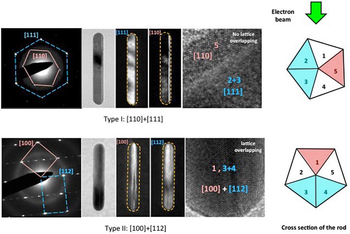
From left to right: electron diffraction, bright-field image, two dark-field images, high-resolution image, and the model of a cross-section of a nanorod with a five-fold twin structure.
What makes working at the CFN worthwhile?
Conducting research using cutting-edge facilities with the most intelligent people in the world on the most advanced nanomaterials and publishing many high-impact papers make working at the CFN worthwhile. This combination is hard to find elsewhere.
If you had to describe the CFN in one word, what would that word be and why?
Wonderful. CFN is wonderful place to do research because of its state-of-the-art equipment and brilliant scientists and users of the facilities. It is nice to work with all these people who are extremely passionate about their work and driven to advance our understanding of nanomaterials.
Where do you see nanomaterials research going in the next 10 years?
It is a very promising and exciting time to work in the nanomaterial field. With the rapid development of nanotechnology, we soon may be able to create many new materials and devices with a vast range of applications in nanomedicine, nanoelectronics, biomaterials, energy production, and consumer products. The CFN’s electron microscopy resources will allow staff and users to be productive and successful in carrying out nanomaterial research.
How did you become interested in studying the structure of nanomaterials?
As a materials scientist, I chose electron microscopy as my PhD training many years ago. I was working on a nanomaterials project and found electron microscopy to be an extremely helpful and straightforward technique for understanding the microstructure and properties of nanomaterials. Since then, I have been studying the structure of nanomaterials by electron microscopy. Exploring the microstructure world of nanomaterials is a truly magical and mysterious experience—I never know what I will discover. This exploration of the unknown is especially true when chemists supply me with nanomaterials that have been subjected to heat or some other type of treatment. It is exciting to study these treated samples because I get to see how the nanomaterials’ structure changes, sometimes in unexpected ways.
2016-6341 | INT/EXT | Newsroom