Nanoscale Structure and Structural Defects in Advanced Materials Group
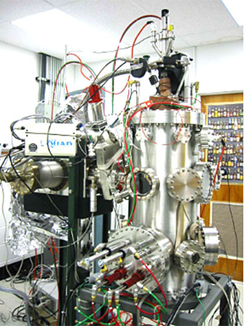
MeV Ultrafast Electron Diffraction System
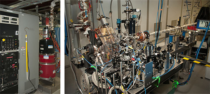
The BNL MeV UED system, developed in 2008-2013, the first of its kind. Left: the Klystron, an amplifier for high RF electric field, and its control system. Right: the overall assemble of the instrument, including individual component of RF gun, solenoid, electron beam diagnostics, sample chamber, RF deflector, and the high-energy electron detector (far right).
The MeV UED system was designed and constructed under the BNL LDRD funding (2008-2013) at the Source Development Lab of NSLS for single-shot pump-probe based ultrafast diffraction experiments, complementary to XFEL. The system was first of its kind. It has a 1.6 cell photocathode RF gun to produce 2 to 5 MeV electrons and a frequency tripled Ti:sapphire laser (266 nm) to generate femtosecond electron pulses. The electron beam diagnostics consist of a movable Faraday cup and a beam profile monitor. The sample chamber has 10 sample slots with cryo-capability and is equipped with a x-y-Φ motorized manipulator (sample requirement is the same as conventional TEM with a 3 mm sample-diameter). Four meters downstream of the diffraction chamber is the high efficiency detector, designed for high energy electrons. The instrument was commissioned in 2012, achievable of a temporal resolution of 120 fs with 106 electrons per pulse, considered as the best at the time in the field. In the past three years, the instrument has been used not only for UED experiments in condensed matter, but also for exploring new capabilities related to both diffraction and imaging, which include developing diagnostic methods for the instrument, improving beam brightness, reducing probe beam size, and boosting acquisition repetition rate from 5 Hz to 50 Hz. We plan to convert the diffraction instrument to an ultrafast electron microscope (UEM), supported by BNL LDRD and DOE SBIR.
- 2-5 MeV electron energy
- 100 fs pulse with 1-50 Hz repetition rate
- 106 electrons per pulse
- 120 fs temporal resolution
- Less than 0.01 % energy spread
- 200 μm beam size on detector
- Synchronization of RF & laser < 50 fs
- Cryogenic capability with 10 sample slots
- Coherence length λL= 1-2 nm, λT = 10 nm
Laser-Free Pulsed Electron Microscopy with GHz excitation
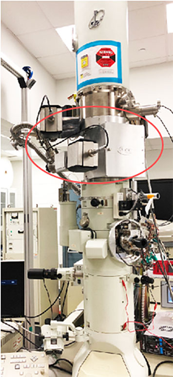
The Pulser system, marked by the red circle, installed on the Lorentz microscope (JEOL 2100F-LM) for RF excitation and stroboscopic ultrafast electron microscopy.
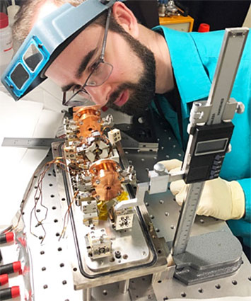
An engineer aligning the RF deflecting cavity in the comb structure of the laser-free electron pulser.
The novel Laser-Free Electron Pulser (LFEP) device was developed in collaboration with Euclid Techlab under four Federal SBIR grants. The development has won the 2019 R&D 100 Award and been granted three US patents for its novelty. The LFEP was successfully installed in our Lorentz microscope in May 2019. The device is based on an electromagnetic-mechanical modulator that consists of two transverse deflecting cavities, three magnetic quadrupoles, and a variable beam aperture. The device modulates and chops the incoming continue-wave (CW) electron beam and transforms it into pico- and sub-picosecond electron pulse sequences, or pulse trains, at an RF repetition rate. The temporal pulse length and rep-rate for the device can be continuously tuned over a wide range with repetition rates from 0.05 GHz up to 12 GHz and a tunable bunch length from tens of ns down to 10ps. The Pulser can be routinely operated in (1) CW mode (i.e. convention TEM operation mode as the microscope itself is not modified, where the electrons from the emission cathode randomly arrive at the sample without resolvable time information), (2) stroboscopic (pump-probe) mode, and (3) pulsed beam mode for radiation sensitive materials. To expand capabilities of the instrument we plan to replace the Lorentz lens with a new high-resolution analytical objective lens, which will allow us to probe samples at much improved spatial resolution for nanostructure characterization, and to tune the magnetic field in the sample area to observe magnetic switching in chiral spin structures.
- Laser-free electron pulse
- Tunable pulse width 10 ps – 50 ns
- Tunable repetition rate 0.05 – 12 GHz
- Instantaneous between three modes (continuous, pulsed, and pump-probe)
Advanced Electron Microscopy Facility
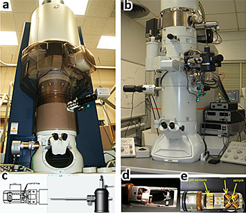
The core research program electron microscopy facility. (a) JEM ARM200CF double-corrected scanning/ transmission electron microscope (S/TEM. (b) The dedicated Lorentz transmission electron microscope (JEM 2100F-LM) with a residual magnetic field smaller than 0.4 mT before its modification as a pulsed microscope. (c) the custom made Gatan low temperature biasing holder, achievable 10 K temperature. (d) home-built Hall probe holder, and (e) Magnetic biasing holder for in-plane field applications.
JEM ARM200CF A New-York-state-owned state-of-the-art electron microscope, JEOL ARM200CF, which was delivered at the end of 2011, and commissioned in June 2013. It is equipped with a cold FEG electron source, two aberration correctors, a Gatan-Quantum electron-energy-loss spectrometer with dual acquisition capabilities, and an SDD x-ray detector. A precession camera was installed in Aug. 2013 for quantitative diffraction measurements. A low-cost direct electron detector (256-pixel x 256-pixel) developed for high-energy physics at CERN (Medipix3, Quantum Detectors) was installed in 2019 for 4D-STEM.
JEM 2100F-LM A special custom-made 200kV FEG TEM that was installed in 2004. Its key feature is the long–focal length objective lens, allowing magnetic measurements at a residual field below 0.4mT with a lattice resolution of 0.5 nm. It is the first of its kind in the US. This microscope was also designed for high-resolution holography of magnetic materials providing fine hologram fringe spacing (<1 nm) and high fringe contrast (50 %). A home-built Hole-Free Phase Plate for magnetic imaging was developed and installed in May 2013. The instrument was modified in May 2019 as a pulsed microscope for GHz excitation and stroboscopic ultrafast microscopy.
Other Capabilities and Resources at BNL
Home-built UHV electron-beam evaporator
UHV Film Deposition System The home-built ultra-high vacuum (UHV) molecular beam epitaxy (MBE) evaporator consists of two 3-kW e-guns. Each gun has three crucibles; 6 target materials loaded into the main chamber at any time. Manual shuttering enables simultaneous deposition of 2 materials from each gun. Base pressure at the main chamber is routinely ~5x10⁻¹⁰ Torr, while deposition pressure is at ~1x10⁻⁹ Torr. High-precision quartz crystal microbalance sensors monitor the thickness of the films. Residual gas partial pressures are monitored with a residual gas analyzer. A resistive heater is installed to maintain elevated substrate temperatures, which are monitored via a thermocouple. The system is mainly used for evaporating films that have nanoscale architectures for studying spin-charge-lattice interactions in topological chiral spin structures and in strongly correlated materials.
Computational Resources The group has purchased and built a high-performance computing clusters to conduct analytical and numerical calculations, including DFT, molecular dynamics and micromagnetic calculations. Over the years we have also developed a suite of computer codes, such as wImage,exe; wBloch.exe; wModel.exe; wMslice.exe, to calculate and simulate electron microscopy images (HREM, STEM-ADF-ABF, SEM), diffractions (PARODI, precession diffraction, electron crystallography and multipole structure refinement), and energy-loss spectra using multislice and Bloch-wave based on dynamic scattering theories. Aspherical electron scattering factors have been derived to take the orbital electrons into account for elements from H to Xe (J. of Appl. Crystallography, 42 1043 (2009)). This unique strength facilitates and reinforces our quantitative analyses of experiment data far beyond those available in commercial software.
Other Accessible Facilities and Recourses at BNL Our group originally built the electron microscopy facility at the Center for Functional Nanomaterials (CFN) and currently have active collaborations with the staffs there. We are also frequent users of CFN’s other facilities including lithography instruments, scanning probes, focused ion beams, and sample preparation equipment. Furthermore, we are heavily involved in the use and development of National Synchrotron Light Source (NSLSII) beam lines, and have productive and ongoing research projects with NSLS staffs on x-ray imaging, diffraction and spectroscopy. These accessible resources at BNL complement our TEM facility for our research, ensuring the proposed research projects can be carried out efficiently and intelligently, and the goals of our program can be achieved.