Integrated Electronics
High-Density Interconnects
The assembly of complex microelectronics requires specialized high-density interconnects. The Instrumentation Department’s High-Density Interconnect and Electronics Assembly (HDI-EA) Laboratory has a multitude of tools for designing and fabricating interconnections—including computer-aided design software and high-tech interconnect equipment—for large international experiments in photon science and particle physics. We also support prototyping and process development for projects in the conceptual stage, with some projects leading to commercial applications.
Our Capabilities
- Application of a variety of interconnect methods, including wire bonding (aluminum wedge and gold ball), gold stud and solder bumping, flip-chip bonding, and precision die bonding
- Protection of wire bonds through encapsulation, underfill, and epoxy dispensing
- Evaluation of the strength and integrity of wire-bonded interconnects via pull and die shear mechanical testing
- Collaboration with the in-house Electronics Assembly Facility, which specializes in the assembly, troubleshooting, repair, cleaning, and deployment of printed circuit boards (PCBs)
- Inspection of interconnects through x-ray imaging to evaluate flip-chip assemblies, ball grid arrays, and PCBs
- Determination of the surface roughness, deposition thickness, and size of detectors, substrates, and bumps via 3-D profilometry with a laser scanning confocal microscope
- Attachment of surface-mount components to PCBs through reflow soldering using automated pick-and-place systems, including those with through-hole technology
- Removal of fluxes, residues, and contaminants from PCBs and substrates by aqueous batch cleaning
- Assembly of custom wires for signal and power cables, including coaxial radio-frequency, multiconductor, cord, ribbon, and flex cables
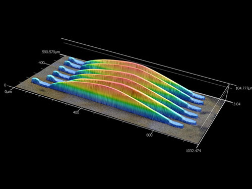
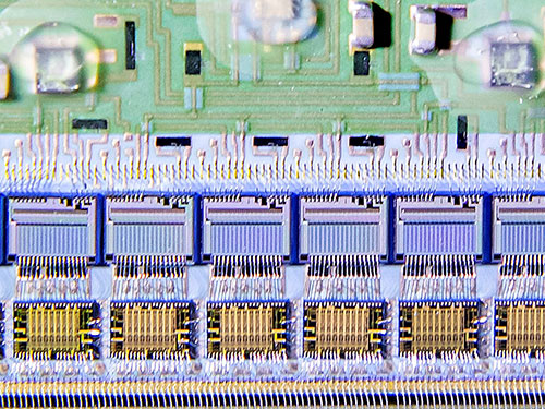
Side view of 25 μm aluminum wire bonds.
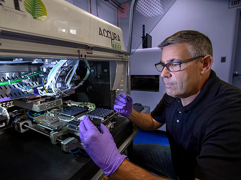
Operating a flip-chip bonder—one of HDI-EA Lab’s high-tech pieces of interconnect equipment—a team member develops a flip-chip process to integrate silicon array sensors with small-pixel application-specific integrated circuits for the development of high-resolution x-ray imagers.
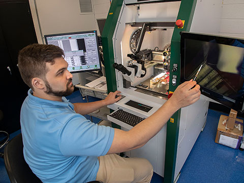
With automated wire bonding equipment, a team member bonds prototype assemblies for the sPHENIX Intermediate Silicon Tracker. The silicon sensors are integrated to application-specific integrated circuits (ASICs) and the ASICs to a signal bus.
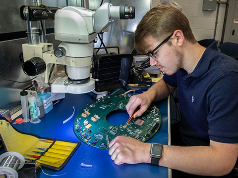
A team member inspects and reworks surface mount technology (components as small as 0.016 × 0.008 inches) for a PCB assembled by the HDI-EA Lab and designed by our in-house PCB Design Group.
Case Studies
Silicon Drift Detectors
CERES Si drift detector.
For the silicon drift detectors (SDDs) invented by our in-house silicon sensor team and initially deployed at CERN for the CERES heavy-ion experiment, we designed the carrier boards for the hybrid electronics and led the detector-readout board integration. Our integrated system design enabled accurate particle tracking for CERES and future experiments at CERN and Brookhaven’s Relativistic Heavy Ion Collider (RHIC).
Silicon Vertex Detector
Silicon vertex detector.
The Silicon Vertex Tracker (SVT) is part of the Solenoidal Tracker at RHIC (STAR). For SVT, we designed and integrated the hybrid front-end electronics with large-area linear SDDs. Our innovative design allowed for a multi-element detector forming a polygon array capable of covering different solid angles to improve particle detection.
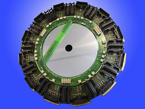
Maia Mircoprobe
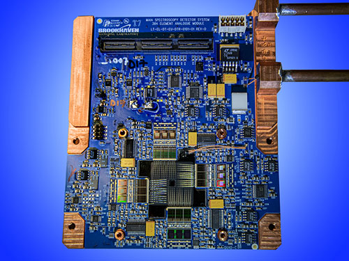
Maia microprobe.
The Maia microprobe is currently in use at Brookhaven’s National Synchrotron Light Source II (NSLS-II), the Cornell High Energy Synchrotron Source (CHESS), DESY, and the Australian Synchrotron. We designed the PCB front-end electronics and contributed to the detector layout for Maia. By optimally placing the wires bonding the 384-detector array to the front-end electronics, we enabled the fast readout of x-ray fluorescence photons for the elemental mapping of materials at these synchrotron beamlines.
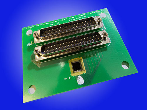
X-ray Beam Position Monitors
NSLS-II x-ray beam position monitor.
High-resolution diamond x-ray beam position monitors developed by our in-house diamond detectors team in collaboration with Stony Brook University are installed at NSLS-II, Argonne’s Advanced Photon Source, CHESS, and other synchrotrons around the world. Our unique assembly and wire bonding capabilities led to designs that allow for novel nonmetallic contact materials, such as ultra-nanocrystalline diamond; small contact geometries; and high-current devices.
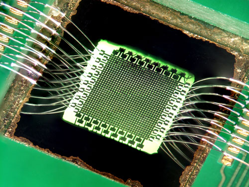
Electronics Integration
Integrated sensor unit.
We integrated the electronics and diamond sensors for transmission-mode diamond x-ray imaging detectors that measure beam shape, position, and flux in real time. These detectors have been deployed at NSLS-II and CHESS.