Facilities and Infrastructure
Fabrication Cleanrooms
For more than 20 years, the Silicon Sensor Fabrication Cleanroom in Brookhaven Lab’s Instrumentation Department has been a main center for the development and production of prototype silicon (Si) radiation sensors. These in-house-developed sensors are being used across the nation and abroad in fields including nuclear and high-energy physics, photon science, and x-ray astronomy.
Our Capabilities
- Application of standard cleanroom techniques, including oxidation and annealing of 4-inch and 6-inch Si wafers with high-temperature furnaces, chemical removal of materials via wet etching, reactive-ion etching, double-sided lithography, sputtering, and rapid thermal processing
- Customization of sensor designs and technology process flows based on application specifications
- Creation of arbitrarily shaped sensors from wafers for specific application needs
- Evaluation of wafers at high voltages while collecting high-accuracy low-current-level measurements
- Collaboration with on-site cleanrooms containing additional processing capabilities, including one dedicated to germanium processing in Brookhaven’s Physics Department and another at the Center for Functional Nanomaterials that can be used for dielectric film depositions and other processes
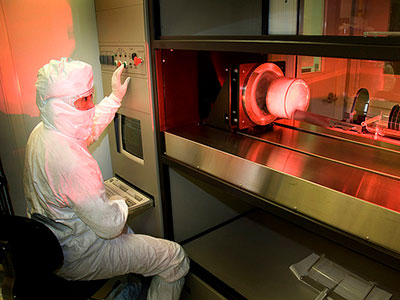
Loading of Si wafers into a furnace for high-temperature annealing and oxidation.
Case Studies
Si Pixel and Strip Sensors
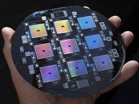
A 4-inch wafer of silicon strips and pixels for photon science experiments.
For photon science and other applications requiring x-ray and charged-particle detection, we developed Si pixel and strip sensors. The Si pixel sensors have been incorporated into the Vertically Integrated Photon Imaging Chip and Hyperspectral Energy X-ray Resolving Imaging Detector, both under development at Brookhaven’s National Synchrotron Light Source II (NSLS-II). The Si strip sensors are supporting x-ray scattering and diffraction experiments at various x-ray synchrotrons, including NSLS-II, the Canadian Light Source, and the Cornell High Energy Synchrotron Source.
Maia Microprobe Pad Sensor
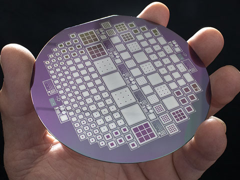
A 6-inch Si wafer of Maia, a 384-channel array of Si diodes for high-rate spectroscopy at synchrotrons.
Our Si pad sensor array for the Maia x-ray microprobe is enabling the high-rate detection of fluorescence x-rays in synchrotron beamlines used for studies in environmental science, biology, nanoscience, and other fields.
Low-gain Avalanche Diodes
A 4-inch silicon wafer populated with LGADs of different sizes.
Our group is one of the few around the world that is developing low-gain avalanche diodes (LGADs), and we are among the first to develop AC-coupled LGADs. Exploiting large signals and fast timing, these sensors could support the detection of soft x-rays for photon science experiments and high-precision measurements of particle arrival times for high-energy physics experiments, including ATLAS and CMS at CERN.