Sensors
Silicon
Brookhaven’s Instrumentation Department has been designing, fabricating, and testing silicon (Si) sensors for nearly 40 years. These sensors support a wide range of applications, including imaging, tracking, and spectroscopy across photon science, high-energy physics, and nuclear physics.
Our Capabilities
- Fabrication of complete sensors—such as strip, pixel, drift, and low-gain avalanche diode sensors—in a class 100 cleanroom
- Design of sensors on 4-inch or 6-inch wafers
- Design of Si charge-coupled device (CCD) sensors, including associated readout and control electronic systems that meet or exceed the state of the art in sensitivity, speed, efficiency, compactness, and power consumption
- Development of thermal and mechanical designs of CCD packages
- Optimization of devices and process flows via technology computer-aided design simulations
- Characterization of sensors at electrical probe stations (current vs. high voltage or capacitance vs. high voltage)
- Characterization of the electro-optic performance of sensors and integrated systems, with troubleshooting of identified performance issues
- Verification of quality control of all assembly and test operations, including fully automated electro-optic test stands with scripted acquisition, analysis, and reporting functions
- Evaluation of CCD electro-optic performance in cryogenic test stands
- Access to a cryogenic probe station at Brookhaven’s Center for Functional Nanomaterials and equipment at other user facilities
- Integration and test of large-format sensor arrays, up to 12 × 12 cm and 144M pixels
- Separation of single sensors from wafers through a laser dicing machine, which enables the cutting of arbitrary shapes, including holes
- Engagement with foundry services from design through testing and procurement of custom sensors
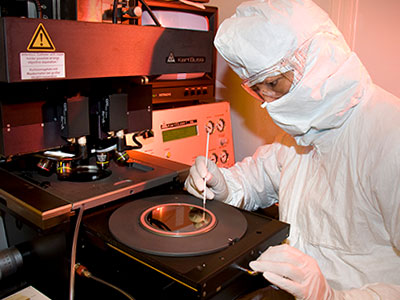
Loading of an Si wafer into a double-sided mask aligner.
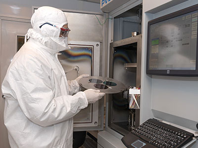
Loading of Si wafers into the sputtering system for aluminum deposition.
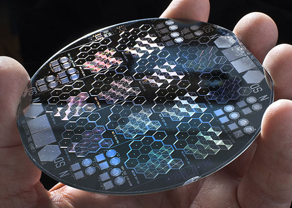
4-inch wafer of silicon strips and pixels for photon science experiments.
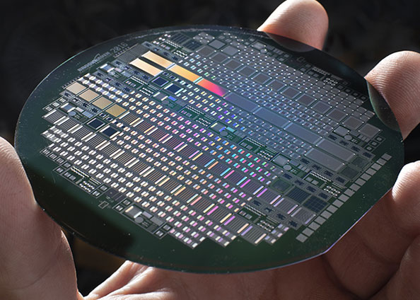
4-inch wafer of Si strip-pixel devices for nuclear physics experiments.
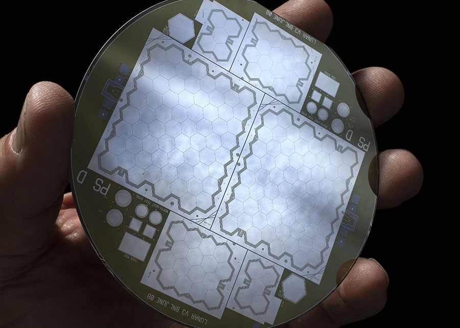
4-inch wafer of very large arrays of spiral Si drift detectors (entrance window side) for astrophysics applications.
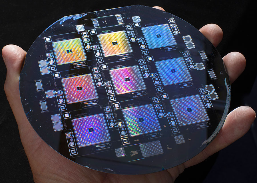
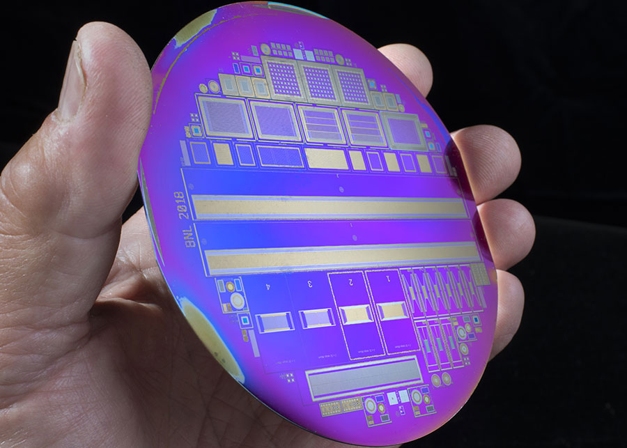
6-inch Si wafer of Maia, a 384-channel array of Si diodes for high-rate spectroscopy at synchrotrons.
4-inch wafer of arrays of spiral Si drift detectors for astrophysics applications.
4-inch wafer of high-voltage vertical Si junction gate field-effect transistors, to be used as switches in high-energy physics experiments.
Case Studies
Drift Detectors
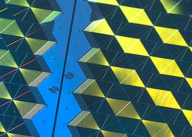
A close-up of an array of spiral Si drift detectors for astrophysics applications.
In 1984, we invented Si drift detectors that were initially deployed in the mid-1990s to provide accurate particle position reconstruction using a limited number of channels for nuclear physics experiments at CERN and Brookhaven’s Relativistic Heavy Ion Collider. Today, these detectors are a mainstay in x-ray spectroscopy for materials science. Our invention opened a new paradigm for charge transport in silicon and established silicon as the material of choice for room-temperature x-ray spectroscopy.
Pixel and Strip Detectors
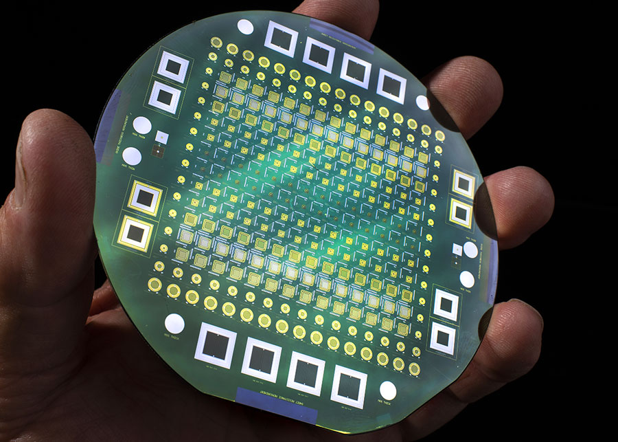
4-inch wafer of an x-ray active matrix pixel sensor for x-ray protein crystallography.
For photon science and other applications requiring x-ray and charged-particle detection, we developed Si pixel and strip sensors. The Si pixel sensors have been incorporated into the Vertically Integrated Photon Imaging Chip and Hyperspectral Energy X-ray Resolving Imaging Detector, both under development at Brookhaven’s National Synchrotron Light Source II (NSLS-II). The Si strip sensors are supporting x-ray scattering and diffraction experiments at various x-ray synchrotrons, including NSLS-II, the Canadian Light Source, and the Cornell High Energy Synchrotron Source.
Low-gain Avalanche Diodes
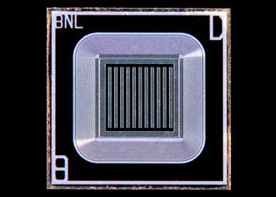
A chip of an AC-coupled low-gain avalanche diode, with metal electrodes patterned as strips.
Our group is one of the few around the world that is developing low-gain avalanche diodes (LGADs), and we are among the first to develop AC-coupled LGADs. Exploiting large signals and fast timing, these sensors could support the detection of soft x-rays for photon science experiments and high-precision measurements of particle arrival times for high-energy physics experiments, including ATLAS and CMS at CERN.
CCD Focal Plane
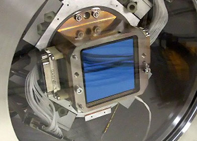
A prototype CCD developed for the Rubin Observatory LSST Camera.
We developed the Rubin Observatory Large Synoptic Survey Telescope (LSST) Camera focal plane of 189 CCDs. This focal plane will detect and convert light from stars and galaxies into electrical signals, from which a computer will reconstruct photos of the night sky with unprecedented detail. These images will be used to study galaxy formation, track asteroids, observe exploding stars, and improve our understanding of dark matter and dark energy.