Facilities and Infrastructure
Micro/Nanofabrication Lab
The Instrumentation Department’s Micro/Nanofabrication Laboratory is dedicated to the design, synthesis, processing, and characterization of components and devices at the micro- and nanoscales. Visiting experimenters are encouraged to actively participate in the design process by learning fundamental fabrication processes such as plasma etching and high-aspect-ratio lithography. Astronomy, particle physics, materials science, and biology are among the fields that we support.
Our Capabilities
- Patterning of materials in our class 100 cleanroom equipped with resist spinners, developing tanks, and etching stations
- Optimization of devices and components through high-resolution structural imaging and chemical microanalysis with scanning electron microscopes (SEMs)
- Access to other instruments at Brookhaven’s user facilities, including SEMs and transmission electron microscopes at the Center for Functional Nanomaterials and x-ray beamlines at the National Synchrotron Light Source II
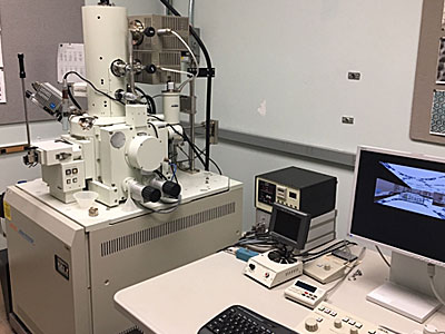
Scanning electron microscope in the Micro/Nanofabrication Laboratory.
Case Studies
Identifying Areas of Damage
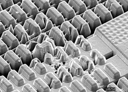
A high-resolution SEM image of a PXL sensor integrated circuit fabricated by plasma etching. The defective areas are visible in the center of the image.
By performing infrared failure analysis, we identified the precise areas of damage in PiXeL (PXL) sensors designed for the STAR nuclear physics experiment at Brookhaven’s Relativistic Heavy Ion Collider (RHIC). This information will guide future designs of the sensor, which will be part of a high-precision tracker probing the conditions of our early universe.
Illuminating CCDs
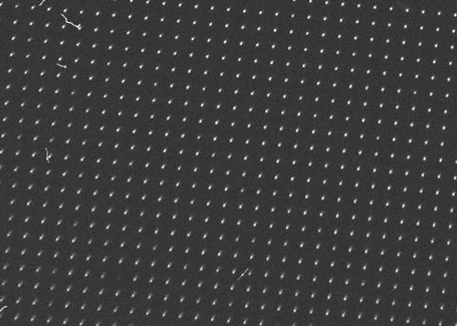
An SEM image of our high-resolution pinhole array fabricated with optical lithography. Despite challenging requirements such as high contrast and low reflectivity, we fabricated 3 μm diameter pinholes with a high degree of accuracy.
Prior to the construction of the final Rubin Observatory Large Synoptic Survey Telescope (LSST) Camera, the optoelectronic performance of the charged-coupled devices (CCDs) making up this camera must be characterized by illuminating the CCD array with a realistic astronomical scene. We fabricated a pinhole array consisting of thousands of artificial stars that will be used to illuminate the CCDs on an optical bench. Ultimately, these characterization studies will help ensure that the LSST Camera—the largest digital camera created to date—can capture wide-field images of the night sky to provide an unparalleled survey of our universe.
Understanding Failure Mechanisms
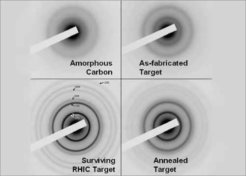
Electron diffraction patterns of amorphous carbon, as-fabricated targets (no annealing), annealed targets, and targets that survived irradiation at RHIC show that carbon “graphitization” occurs and can be simulated by heating the targets.
Carbon targets fabricated by electron-beam evaporation typically fail after only a few hours of being irradiated by the 200 GeV proton beam at RHIC. To understand the failure mechanism, we carried out electron diffraction studies, which revealed that target heating during beam exposure results in a crystalline structure transformation from amorphous carbon to graphene. Now, we are determining the precise time-temperature annealing cycle for optimizing material properties to extend target lifetimes.