Scientists Set Record Resolution for Drawing at the One-Nanometer Length Scale
An electron microscope–based lithography system for patterning materials at sizes as small as a single nanometer could be used to create and study materials with new properties
April 28, 2017
 enlarge
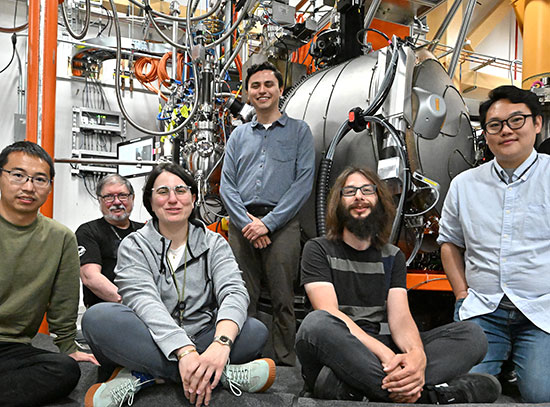
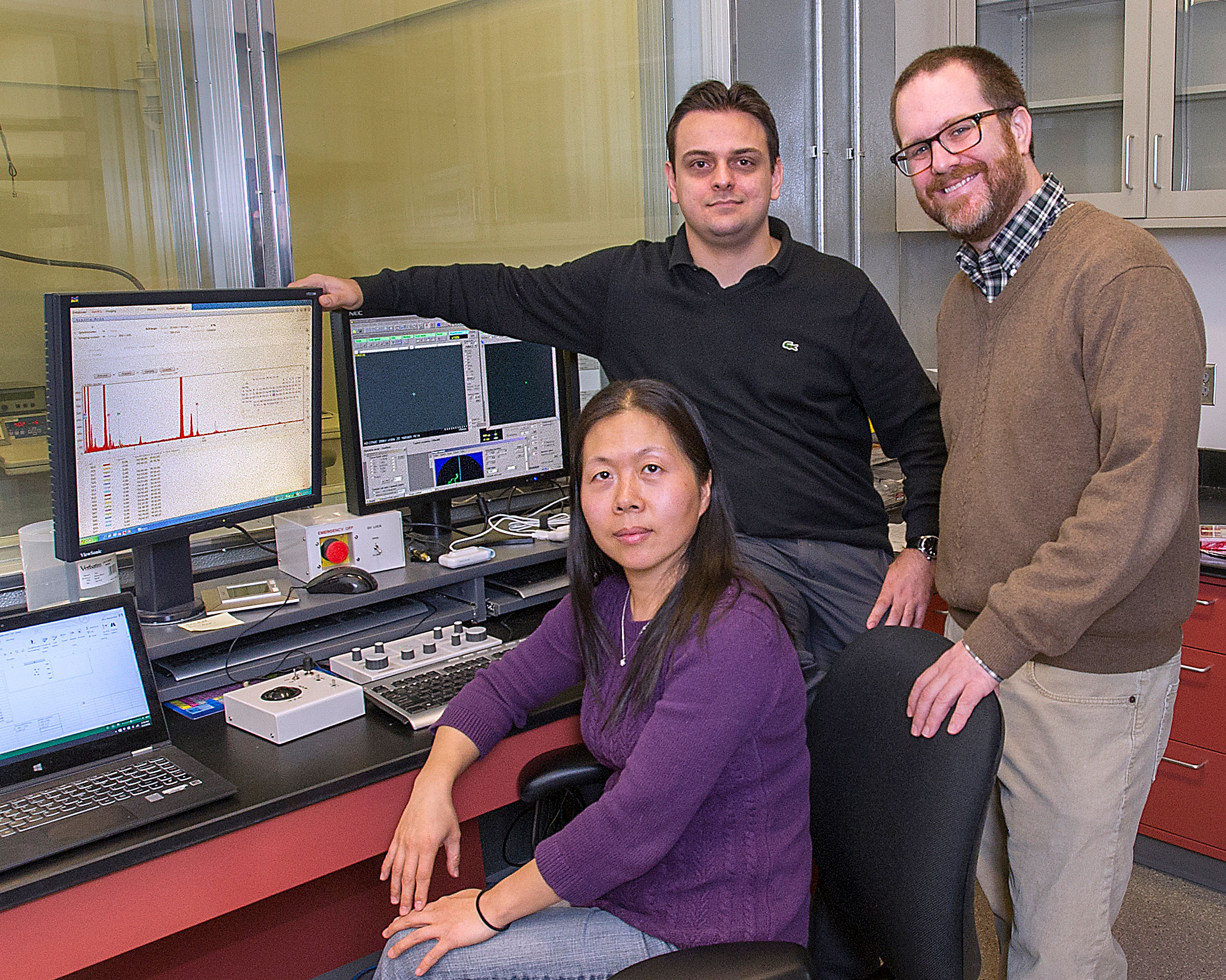
(Left to right) Lihua Zhang, Vitor Manfrinato, and Aaron Stein are part of the team at Brookhaven Lab's Center for Functional Nanomaterials that pushed the resolution limits of electron-beam lithography—a technique for creating nanoscale patterns—to the one-nanometer length scale. Team members not pictured are Chang-Yong Nam, Kevin Yager, Eric Stach, and Charles Black.
UPTON, NY—The ability to pattern materials at ever-smaller sizes—using electron-beam lithography (EBL), in which an electron-sensitive material is exposed to a focused beam of electrons, as a primary method—is driving advances in nanotechnology. When the feature size of materials is reduced from the macroscale to the nanoscale, individual atoms and molecules can be manipulated to dramatically alter material properties, such as color, chemical reactivity, electrical conductivity, and light interactions.
In the ongoing quest to pattern materials with ever-smaller feature sizes, scientists at the Center for Functional Nanomaterials (CFN)—a U.S. Department of Energy (DOE) Office of Science User Facility at Brookhaven National Laboratory—have recently set a new record. Performing EBL with a scanning transmission electron microscope (STEM), they have patterned thin films of the polymer poly(methyl methacrylate), or PMMA, with individual features as small as one nanometer (nm), and with a spacing between features of 11 nm, yielding an areal density of nearly one trillion features per square centimeter. These record achievements are published in the April 18 online edition of Nano Letters.
“Our goal at CFN is to study how the optical, electrical, thermal, and other properties of materials change as their feature sizes get smaller,” said lead author Vitor Manfrinato, a research associate in CFN’s electron microscopy group who began the project as a CFN user while completing his doctoral work at MIT. “Until now, patterning materials at a single nanometer has not been possible in a controllable and efficient way.”
Commercial EBL instruments typically pattern materials at sizes between 10 and 20 nanometers. Techniques that can produce higher-resolution patterns require special conditions that either limit their practical utility or dramatically slow down the patterning process. Here, the scientists pushed the resolution limits of EBL by installing a pattern generator—an electronic system that precisely moves the electron beam over a sample to draw patterns designed with computer software—in one of CFN’s aberration-corrected STEMs, a specialized microscope that provides a focused electron beam at the atomic scale.
“We converted an imaging tool into a drawing tool that is capable of not only taking atomic-resolution images but also making atomic-resolution structures,” said coauthor Aaron Stein, a senior scientist in the electronic nanomaterials group at CFN.
 enlarge
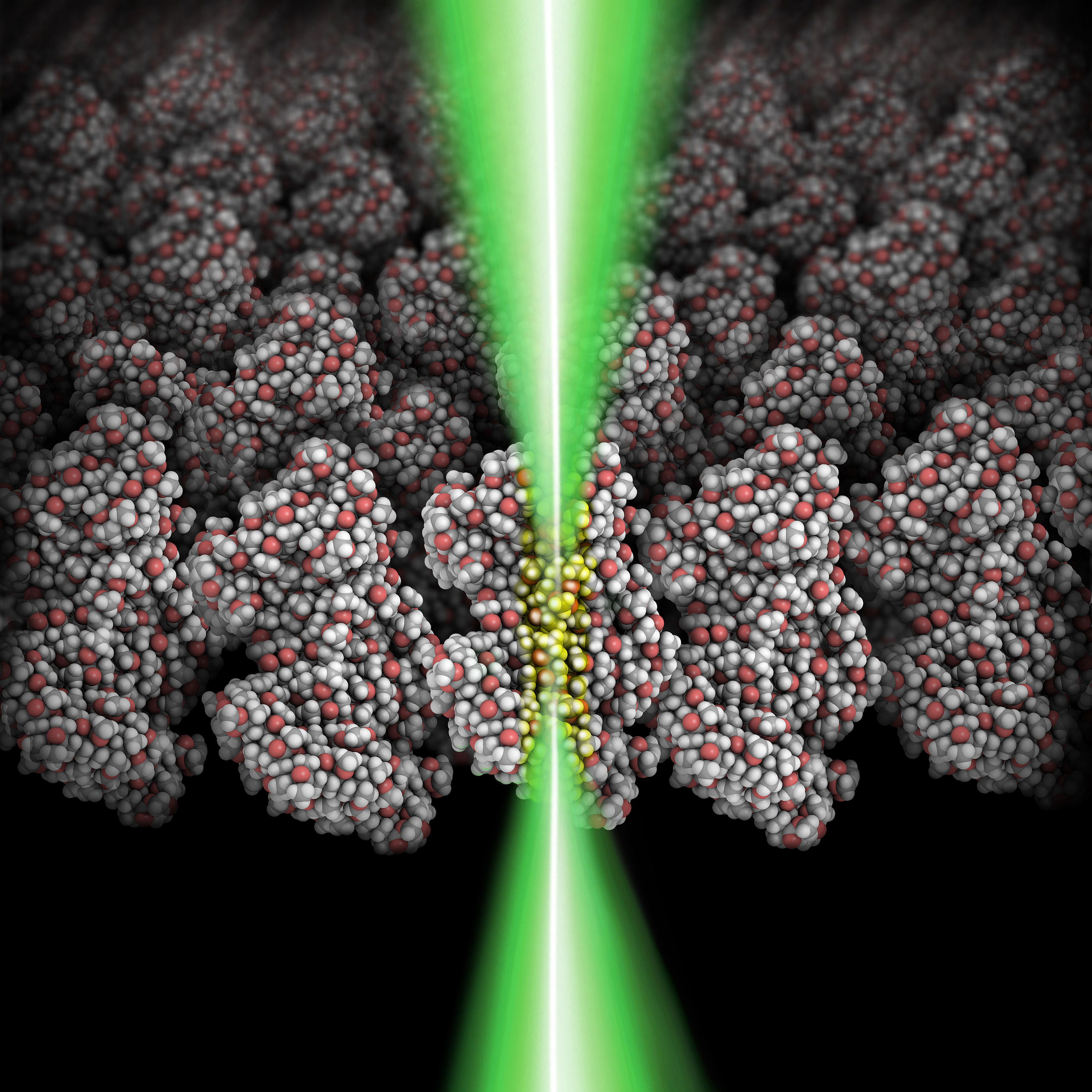
A schematic showing a focused electron beam (green) shining through a polymeric film (grey: carbon atoms; red: oxygen atoms; white: hydrogen atoms). The glowing area (yellow) indicates the molecular volume chemically modified by the focused electron beam.
The team’s patterned PMMA films can be used as stencils for transferring the drawn single-digit nanometer feature into any other material. In this work, the scientists created structures smaller than 5 nm in both metallic (gold palladium) and semiconducting (zinc oxide) materials. Their fabricated gold palladium features were as small as six atoms wide.
Despite this record-setting demonstration, the team remains interested in understanding the factors that still limit resolution, and ultimately pushing EBL to its fundamental limit.
“The resolution of EBL can be impacted by many parameters, including instrument limitations, interactions between the electron beam and the polymer material, molecular dimensions associated with the polymer structure, and chemical processes of lithography,” explained Manfrinato.
An exciting result of this study was the realization that polymer films can be patterned at sizes much smaller than the 26 nm effective radius of the PMMA macromolecule. “The polymer chains that make up a PMMA macromolecule are a million repeating monomers (molecules) long—in a film, these macromolecules are all entangled and balled up,” said Stein. “We were surprised to find that the smallest size we could pattern is well below the size of the macromolecule and nears the size of one of the monomer repeating units, as small as a single nanometer.”
Next, the team plans to use their technique to study the properties of materials patterned at one-nanometer dimensions. One early target will be the semiconducting material silicon, whose electronic and optical properties are predicted to change at the single-digit nanometer scale.
“This technique opens up many exciting materials engineering possibilities, tailoring properties if not atom by atom, then closer than ever before,” said Stein. “Because the CFN is a national user facility, we will soon be offering our first-of-a-kind nanoscience tool to users from around the world. It will be really interesting to see how other scientists make use of this new capability.”
This work is supported by DOE’s Office of Science.
Brookhaven National Laboratory is supported by the Office of Science of the U.S. Department of Energy. The Office of Science is the single largest supporter of basic research in the physical sciences in the United States, and is working to address some of the most pressing challenges of our time. For more information, please visit science.energy.gov.
2017-12189 | INT/EXT | Newsroom