New Dual-Beam Microscope Installed at the Center for Functional Nanomaterials
The multifunctional, latest-generation tool—which combines an electron and ion beam and is equipped with advanced capabilities for precise machining and sample characterization of nanomaterials—is now available to users
May 18, 2021
 enlarge
A view of the inside of the Helios G5 dual-beam microscope main chamber. The system, now available to users of the Center for Functional Nanomaterials at Brookhaven Lab, is loaded with a variety of imaging capabilities and analysis detectors.
Every year, the Center for Functional Nanomaterials (CFN)—a U.S. Department of Energy (DOE) Office of Science User Facility at Brookhaven National Laboratory—welcomes close to 600 users. At the CFN, users can request access to a broad range of tools for researching materials spanning mere billionths of a meter and making functional devices from them. As a material becomes smaller, transforming from its larger “bulk” size to these nanoscale dimensions, its electronic, chemical, and other properties change. Scientists are actively exploring how the nanoscale versions of materials behave in order to leverage them for specific applications.
One instrument available at the CFN—the dual-beam scanning electron microscope (SEM)/focused-ion beam (FIB), which is located in the Nanofabrication Facility—can simultaneously prepare and analyze nanomaterial samples. Because of its unique capability, the dual-beam tool has been in high demand by users year after year.
“It’s a dual microscope—dual because it uses electron and ion beams,” explained tool manager Fernando Camino, a staff scientist in the CFN Electron Microscopy Group. “One beam contains electrons for imaging. The other beam contains ions, or electrically charged atoms, which can also be used for imaging. But ions are very heavy, so they can be focused onto a sample at precise locations to mill desired shapes at the same time they are imaging.”
Conventionally, the dual-beam SEM/FIB has been useful for editing circuits and analyzing failure spots in microelectronics. With this tool, microelectronics engineers can “surgically” go to the layer containing the failure area, obtain cross-section images to visualize and understand what’s happening, and fix the problem.
 enlarge
Kim Kisslinger (standing) and Fernando Camino testing one of the many capabilities of the new dual-beam tool.
The utility of the dual-beam SEM/FIB has since expanded into other application areas. For example, at the CFN, scientists routinely use the tool to make high-quality samples for transmission electron microscopes (TEMs), leveraging the expertise of Kim Kisslinger, an in-house expert in TEM sample preparation.
In the 10 years the CFN dual-beam SEM/FIB has been operating, it’s supported many user projects. In 2019, more than 40 research studies citing its use were published. Recognizing the tool’s importance in enabling nanoscience and seeking to leverage technological advances implemented by the manufacturer over the years, the CFN decided it was time to upgrade this first-generation “Helios” system (Helios G1) to the fifth generation, Helios G5. Manufactured by Thermo Fisher Scientific, Helios G5 is the latest and most-advanced generation to date.
“This machine is one of only a few open to the scientific community,” said Camino. “At the CFN, we not only provide users with this very sophisticated tool but also train them on how to use it for their research.”
The Helios G5 improves several existing capabilities and specifications, as compared to the Helios G1 originally installed at the CFN. For example, the ion beam current is three times higher, accelerating bulk milling. The FIB imaging resolution at low energies (below 2 keV) is two times higher, enabling users to prepare TEM samples of better quality.
The Helios G5 also features completely new capabilities. One of the major improvements is the automation of the TEM sample preparation capability. Now, users can perform fully automated, unattended (overnight), multi-site bulk milling of initial TEM samples and automated final thinning of these samples.
The Helios G5 also addresses an important problem arising when scientists make TEM samples. In order for electrons to pass through them, these samples must be very thin (around 50 nanometers or less). As the FIB mills a material to the necessary thickness, the material’s surface becomes damaged. For example, suppose the material is a crystal, meaning it has a well-ordered arrangement of atoms. The surface of the side being milled can become amorphous, or lose its crystalline structure.
The highest-quality samples result when the surface is “cleaned” with low-energy ions. However, in the old tool, at these low energies, the imaging resolution was poor. Therefore, pinpointing which areas required cleaning was difficult.
With the new tool, scientists can see samples at low energy thanks to the improved ion optics of the new FIB column. They can also further improve sample quality with a new polishing capability.
“Milling creates some damage we can’t avoid,” explained Camino. “The Helios G5 can do a very fine polishing with argon gas to reduce this unavoidable damage and produce the best samples possible.”
Milling is especially damaging to biological and other beam-sensitive materials. Because the ions are heavy and accelerated to high energies for milling, they generate heat. This heat can damage samples, more so if they are made of soft matter. To help prevent this heat-induced damage, the new system incorporates a “cold” sample stage for milling at low temperatures.
The scientific community will also benefit from a new “slice and view” software for automatically creating three-dimensional (3-D) images. The software acquires data by milling serial sections (slices) of a sample with the FIB and then imaging each slice.
“We slice, take a picture of the section we sliced, then slice a little deeper, take another picture, and so on,” explained Camino. “The software reconstructs all these two-dimensional images at different depths to recreate the 3-D volume of the sample.”
 enlarge
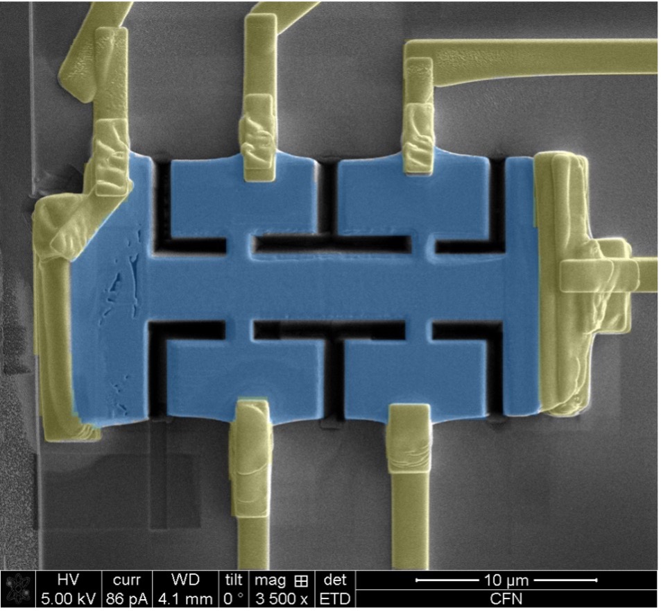
A Hall bar device fully fabricated inside the Helios G5 from a bulk crystal (a collaboration with Cedomir Petrovic's group at Brookhaven). The electron backscatter diffraction detector in the new system will allow users to identify crystallographic planes to guide the fabrication of devices designed to measure electronic transport along specific crystal orientations.
Beyond imaging, Helios G5 offers enhanced detectors for sample analysis. Conventionally, the tool has been equipped with an x-ray detector for identifying the chemical composition of a sample. Now, it also features an electron backscatter diffraction detector, whose signals encode a sample’s crystal orientation. Determining crystal orientation is especially important for quantum or topological materials. Characterizing these kinds of samples can require making electrical transport measurements along specific orientations of the crystal. The electronic properties can be very different depending on which direction they are measured relative to the crystal axis.
“The electron backscatter diffraction detector allows us to see a sample’s crystal orientation, while the FIB allows us to cut slices any which way we want, whether vertically, horizontally, or some other direction,” said Camino. “More than that, once we cut and shape the crystal, we can put it on a substrate with electrical contacts to measure its transport characteristics. So, inside this single machine, we can make full devices out of bulk crystals.”
“Nanorobots” are another new measurement capability of the Helios G5. These tiny needle-like probes move piezoelectrically. Piezoelectricity is a phenomenon in which an electrical voltage appears when a material is subjected to some sort of mechanical stress, like squeezing or stretching. Using the SEM at high resolution, scientists can precisely position these probes on a material of interest—say a nanowire, a long wire-shaped nanostructure. By touching the ends of the nanowire to the probes, scientists can measure its electrical properties.
“The Helios G5 is highly versatile, and we are always seeking opportunities to go beyond the intended uses of the tool,” said Camino. “For example, making devices is not something the manufacturer publicizes, but we see it as a useful capability. We’re excited to open up this latest-generation tool to users and expand the scope of applications.”
If you have questions about the Helios G5, contact Fernando Camino at (631) 344-7606 or fcamino@bnl.gov. Interested in becoming a CFN user? Submit a proposal through the CFN Proposal Portal. The next deadline is May 31. If you have questions about using CFN facilities or partnering with CFN scientists, please contact CFN Assistant Director for Strategic Partnerships Priscilla Antunez at (631) 344-6186 or pantunez@bnl.gov.
Brookhaven National Laboratory is supported by the U.S. Department of Energy’s Office of Science. The Office of Science is the single largest supporter of basic research in the physical sciences in the United States and is working to address some of the most pressing challenges of our time. For more information, visit https://energy.gov/science.
Follow @BrookhavenLab on Twitter or find us on Facebook.
2021-18735 | INT/EXT | Newsroom