Silicon Ally: Penn Engineers Grow Full Wafers of High-Performing 2D Semiconductor That Integrates With State-of-the-Art Chips
October 6, 2023
By Devorah Fischler, University of Pennsylvania
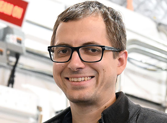
Researchers at the University of Pennsylvania School of Engineering and Applied Science have grown a high-performing 2D semiconductor to a full-size, industrial-scale wafer. In addition, the semiconductor material, indium selenide (InSe), can be deposited at temperatures low enough to integrate with a silicon chip. (Pictured above: Seunguk Song)
The following article was originally issued by the University of Pennsylvania School of Engineering and Applied Science. This research used the electron microscopy resources of the Center for Functional Nanomaterials (CFN). CFN is a U.S. Department of Energy (DOE) Office of Science User Facility at DOE’s Brookhaven National Laboratory. For more information on Brookhaven’s role in this research, contact Denise Yazak (dyazak@bnl.gov, 631-344-6371).
The semiconductor industry today is working to respond to a threefold mandate: increasing computing power, decreasing chip sizes and managing power in densely packed circuits.
To meet these demands, the industry must look beyond silicon to produce devices appropriate for the growing role of computing.
While unlikely to abandon the workhorse material anytime in the near or distant future, the technology sector will require creative enhancements in chip materials and architectures to produce devices appropriate for the growing role of computing.
One of the biggest shortcomings of silicon is that it can only be made so thin because its material properties are fundamentally limited to three dimensions [3D]. For this reason, two-dimensional [2D] semiconductors — so thin as to have almost no height — have become an object of interest to scientists, engineers and microelectronics manufacturers.
Thinner chip components would provide greater control and precision over the flow of electricity in a device, while lowering the amount of energy required to power it. A 2D semiconductor would also contribute to keeping the surface area of a chip to a minimum, lying in a thin film atop a supporting silicon device.
But until recently, attempts to create such a material have been unsuccessful.
Certain 2D semiconductors have performed well on their own, but required such high temperatures to deposit they destroyed the underlying silicon chip. Others could be deposited at silicon-compatible temperatures, but their electronic properties — energy usage, speed, precision — were lacking. Some fit the bill for temperature and performance but could not be grown to the requisite purity at industry-standard sizes.
Now, researchers at the University of Pennsylvania School of Engineering and Applied Science have grown a high-performing 2D semiconductor to a full-size, industrial-scale wafer. In addition, the semiconductor material, indium selenide (InSe), can be deposited at temperatures low enough to integrate with a silicon chip.
Deep Jariwala, Associate Professor and Peter and Susanne Armstrong Distinguished Scholar in the Department of Electrical and Systems Engineering (ESE), and Seunguk Song, postdoctoral fellow in ESE, led the study, published recently in Matter.
“Semiconductor manufacturing is an industrial-scale manufacturing process,” says Jariwala. “You aren’t going to have a viable material unless you can produce it on industrial-scale wafers. The more chips you can make in a batch, the lower the price. But the material must also be pure to ensure performance. This is why silicon is so prevalent — you can make it in large quantities without sacrificing purity.”
InSe has long shown promise as a 2D material for advanced computing chips because it carries electrical charge exceptionally well. But producing large enough films of InSe has proven tricky because the chemistry of indium and selenium tends to combine in a few different molecular proportions, taking on chemical structures with varying ratios of each element and thus compromising its purity.
The team’s success hinged on Song’s application of a growth technique that overcame the quirks of InSe’s atomic structure.
“For the purposes of an advanced computing technology, the chemical structure of 2D InSe needs to be exactly 50:50 between the two elements. The resulting material needs a uniform chemical structure over a large area to work,” says Song.
The team achieved this groundbreaking purity using a growth technique called “vertical metal-organic chemical vapor deposition” (MOCVD). Previous research had attempted to introduce the indium and selenium in equal quantities and at the same time. Song demonstrated, however, that this method was the source of undesirable chemical structures in the material, producing molecules with varying ratios of each element. MOCVD, by contrast, works by sending the indium in a continuous stream while introducing the selenium in pulses.
“By pulsing, you give the indium and selenium time to combine. In the moments between pulses, you deprive the environment of selenium, which prevents the ratio from getting too high. The benefit of the pulse is the pause. That’s how we get a uniform 50:50 ratio across our entire full-size wafer,” says Song.
In addition to chemical purity, the team was also able to control and align the direction of crystals in the material, enhancing the quality of their semiconductor even further by providing a seamless environment for electron transport.
“The two most important material qualities in a semiconductor are chemical purity and crystalline order. The most important industrial quality is scalability. This material checks every box,” says Jariwala.
2023-21492 | INT/EXT | Newsroom


