Seeking New Physics in Atomically Thin Materials with Abdullah Al-Mahboob
interview with a CFN Staff Scientist
June 26, 2024
Abdullah Al-Mahboob is a scientist in the Interface Science and Catalysis group at the Center for Functional Nanomaterials (CFN) and uses the resources of the National Synchrotron Light Source II; both are U.S. Department of Energy (DOE) Office of Science user facilities at DOE’s Brookhaven National Laboratory. A longtime CFN user prior to joining the CFN staff in 2022, Al-Mahboob is using cutting-edge tools at both facilities to study the properties of ultra-thin layered materials with interesting electronic and optical properties.
What kind of materials do you study at CFN?
One of my goals as a CFN staff scientist is to develop new 2D quantum materials. I study transition metal dichalcogenides (TMDs), which are 2D quantum materials that consist of a transition metal layer, such as molybdenum or tungsten, between two layers of a chalcogen, such as sulfur or selenium. This configuration is called a heterostructure and is essentially 2D because the layers are atomically thin. These 2D materials can behave in very interesting and potentially useful ways.
I am particularly interested in how energy and charge transfer between the layers. How is this affected by the spacing between the layers? What happens when they are excited with light? TMDs are a playground for exploring new physics, such as new quantum optical properties. They could have an important role in new technologies.
What kind of new behaviors can result from this configuration?
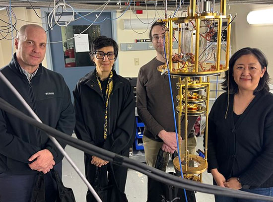
One thing we have been studying, in a collaboration with colleagues at the University of Warsaw in Poland, is what happens when a material with a small energy band gap is stacked with a material that has a large energy band gap. The band gap defines how much energy is needed for valence electrons to become conduction electrons.
In this case, energy can transfer from the lower-energy band gap material to the higher-energy band gap material when the system is excited. For example, in certain conditions, we see that the lower-energy band gap material can absorb light and transfer it to the other material. When you have atomically thin layers and increase the distance between the layers within a range of, typically, just a few nanometers, the energy transfer first increases and then starts to decrease. This is a new phenomenon that we are trying to understand, such as by trying out different combinations of 2D materials and looking at how their structures affect the energy transfer.
What research tools do you use?
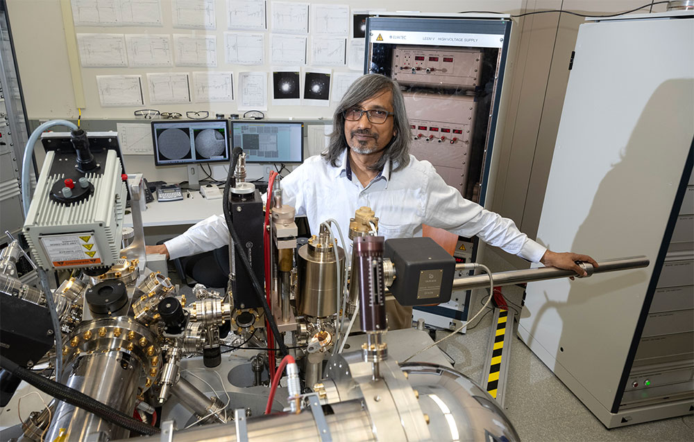
My expertise is in spectro-microscopy tools, such as electron microscopy and photo-electron microscopy, which are available at CFN. I also rely on low energy electron microscopy and X-ray photoemission electron microscopy, which are two techniques available at the NSLS-II Electron Spectro-Microscopy (ESM) beamline. By combining the methods available at the two facilities, we can study our samples’ properties in real time.
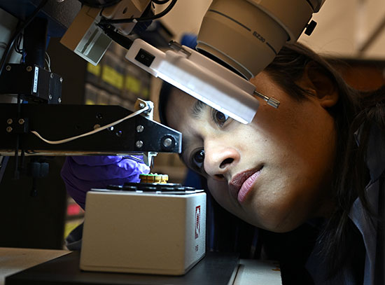
I also use CFN’s Quantum Material Press, or QPress, which is a robotic, automated system for creating heterostructures. Previously, we had to create samples by using Scotch tape to manually “lift” layers off a bulk sample. This was a difficult process, and you might make many samples and only get one that is right. With the QPress, the process is much quicker, and the samples yielded are of much higher quality. I can get my samples prepared in a day, versus a few days. The QPress provides you with the ability to control the rotation and tilt of the layers, as well.
What else are you studying right now?
Currently, I am developing new phases of 2D silicon materials, which is a separate project from my TMD research. Ultimately, I would like to combine existing silicon technologies with new 2D silicon-based materials to yield new technologies.
Another collaboration we are doing with the University of Warsaw is studying samples fabricated from TMDs that are bilayer materials. We are seeing that there is immediate charge transfer between the layers. We are also looking at how the substrate affects the charge transfer. For example, one substrate we use is sapphire because TMDs can be grown epitaxially on sapphire, which means that the TMD layer grows in a way that is directed by the molecular structure of the sapphire.
Other substrates that we are experimenting with are copper, ruthenium, and quartz. Depending on what kind of measurements we want to do, we pick the substrate accordingly. Quartz, for example, is optically inert, meaning it doesn’t change the properties of incoming light. That makes it appropriate for optical experiments.
What is a typical week like for you at CFN?
A few days a week, I have meetings with users. I also have students working with me, so I have to make time for them. Otherwise, it is a relaxed schedule. However, as a scientist at a user facility, I cannot use the instruments whenever I want. I have to submit and use my own user proposal time, or I can come in on the weekend or at night when we need extra time beyond what our proposal gives us. Sometimes, I even work throughout the night. I try to use the tools as much as possible.
Brookhaven National Laboratory is supported by the Office of Science of the U.S. Department of Energy. The Office of Science is the single largest supporter of basic research in the physical sciences in the United States and is working to address some of the most pressing challenges of our time. For more information, visit science.energy.gov.
Follow @BrookhavenLab on social media. Find us on Instagram, LinkedIn, X, and Facebook.
2024-21979 | INT/EXT | Newsroom


