Rare & Efficient Energy Transfer in 2D Heterostructures
August 30, 2023
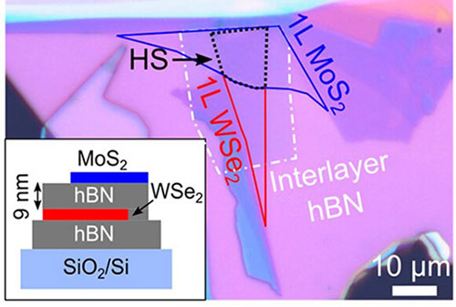
Optical image of the stacked 2D material heterostructure, with different layers outlined for clarity. Inset is the schematic cross-sectional illustration of the sample.
Scientific Achievement
CFN staff and users co-led a study that discovered an efficient and unusual energy transfer process from a lower to higher bandgap semiconductor material in stacked heterostructures of monolayer WSe2 & MoS2. This unconventional process enhances photoluminescence from the heterostructure, compared to that from the MoS2 monolayer alone.
Significance and Impact
This work illuminates pathways to increasing quantum efficiency in Transition Metal Dichalcogenide 2D materials, which have favorable properties for optoelectronic and photovoltaic applications.
Research Details
Atomically thin two dimensional materials exhibit many extraordinary phenomena in comparison to their corresponding bulk materials. Heterostructures (HS) made of Transition-Metal Dichalcogenide (TMD) monolayers (ML) have potential optoelectronic and photovoltaic applications since the energy gaps in these materials cover a wide range of the solar spectrum. Quantum quasiparticles, like excitons, electrons bound to electron holes, play novel roles in the optoelectronic properties of TMD ML due to their interesting spin-resolved energy landscapes. The quantum field mediated excitonic exchange processes can be explored by probing novel optoelectronic characteristics if the thermally activated process is suppressed. Scientists at CFN and their collaborators at the University of Warsaw studied the quantum field mediated energy transfer process between the layers of TMDs separated by noninteracting nanoscale media. The work reveals an unconventional interlayer energy transfer (ET) process in the TMD heterostructures.
The team studied the effect of resonant overlaps between the high-lying excitonic states of WSe2 and MoS2 monolayers (ML) at the interlayer ET process with a few nm-thick hexagonal boron nitride (hBN), a charge-blocking layer. Both of these TMD materials have overlapping higher energy B and C (MoS2)/D (WSe2) absorption features. The matching energy of excitations at the WSe2 B and D absorption regions results in MoS2 PL enhancement in the heterostructure (HS) area due to the interlayer ET process from the WSe2-to-MoS2 layer. This type of ET process from the lower-to-higher optical bandgap material is not typical in the TMD HSs, since ET conventionally happens from the higher-to-lower bandgap materials.
The observed PL enhancement and underlying optoelectronic pathways for excitonic exchange are from ML WSe2 to MoS2. Photoluminescence excitation (PLE) maps are taken at 8 K to Room temperature. Competing interlayer charge transfer (CT) and energy transfer (ET) processes control the photocarrier relaxation pathways in TMD heterostructures (HSs). In TMDs, long-distance ET can survive up to several tens of nm, unlike the CT process. This work shows that an efficient ET occurs from the 1Ls WSe2-to-MoS2 with an interlayer hBN due to the resonant overlapping of the high-lying excitonic states between the two TMDs, resulting in enhanced HS MoS2 PL emission. With increasing temperature, the ET process becomes weaker due to the increased electron–phonon scattering, destroying the enhanced MoS2 emission. The work provides new insight into the long-distance ET process and its effect on the photocarrier relaxation pathways.
In this work, scientists employed multiple optical spectroscopic techniques at cryogenic temperatures, such as µ-PL, µ-photoluminescence excitation (PLE) at the University of Warsaw, and differential reflectance contrast (RC), which were complemented by the density functional theory (DFT) calculation of band structures to study the ET process.
- A nanoscale layer of insulating hBN separated the stacked WSe2 and Mo52 monolayers.
- Sample preparation was enabled by the CFN Quantum Material Press (QPress).
CFN Capabilities: The CFN Materials Synthesis & Characterization Facility was used for the QPress robotic exfoliator and stacker of 2D materials.
Publication Reference
Karmakar A., Kazimierczuk T., Antoniazzi I., Raczynski M., Park S., Jang H., Taniguchi T., Watanabe K., Babinski A., Al-Mahboob A., Molas M.R. “Excitation-Dependent High-Lying Excitonic Exchange via Interlayer Energy Transfer from Lower-to-Higher Bandgap 2D Material.” Nano Letters 23, 5617 (2023).
DOI: https://doi.org/10.1021/acs.nanolett.3c01127
OSTI: https://www.osti.gov/biblio/1988604
Brookhaven Newsroom: Making Big Leaps in Understanding Nanoscale Gaps
2023-21454 | INT/EXT | Newsroom