Brookhaven Lab and Small Business Partner to Advance Characterization Tools
Center for Functional Nanomaterials scientists offer their expertise in performing experiments under controlled temperatures and pressures to develop environmental cells for high-resolution photothermal infrared imaging and spectroscopy instruments
November 10, 2021
 enlarge
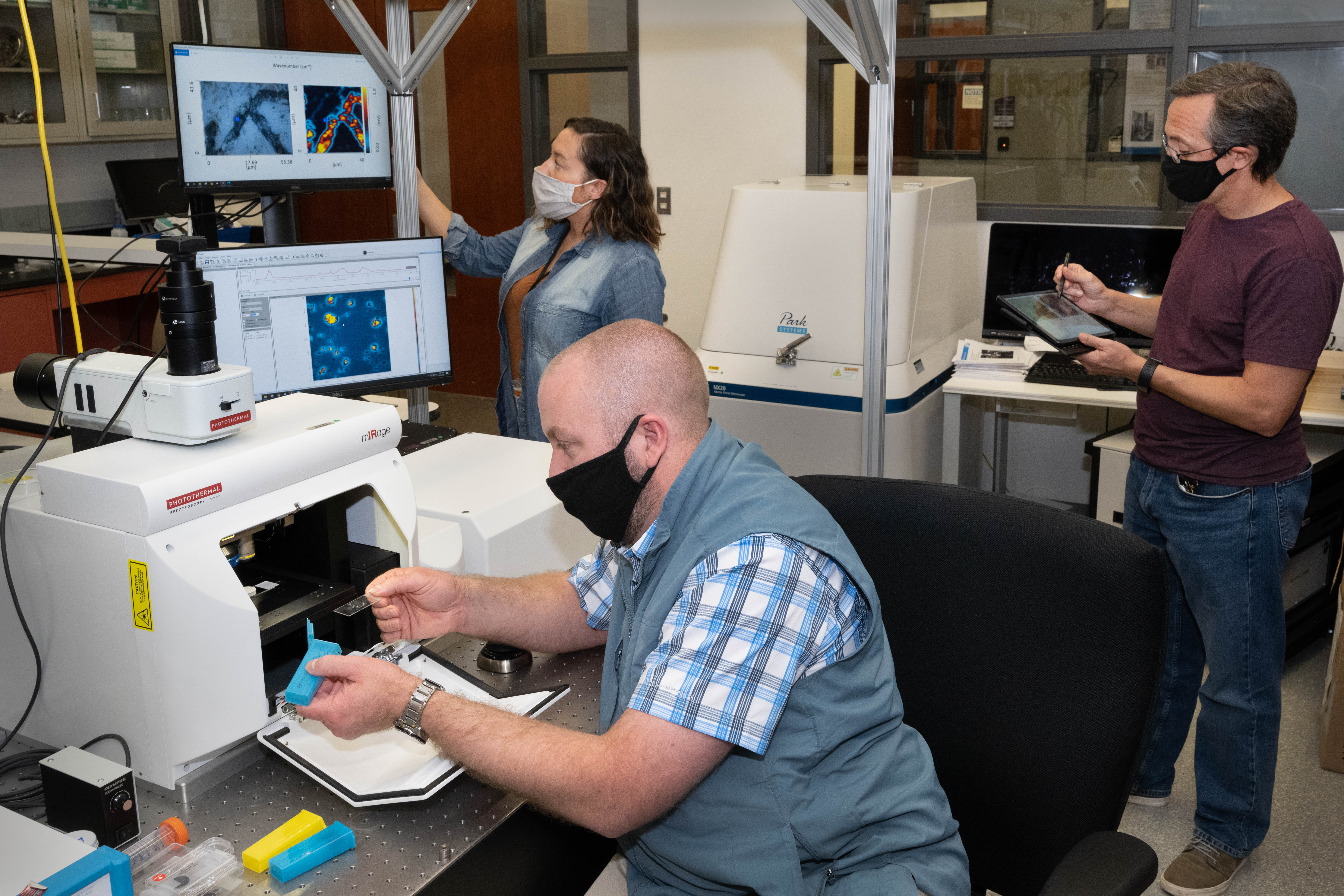
Samuel Tenney (sitting front), Sabine Neal (standing near screens), and Dario Stacchiola at the Center for Functional Nanomaterials with an instrument capable of infrared and Raman spectroscopy. The team is developing an environmental cell for this instrument to enable the study of nanomaterials in operating conditions.
The U.S. Department of Energy (DOE) Office of Science maintains and operates 28 scientific user facilities at national laboratories across the country. These national user facilities provide researchers worldwide with advanced tools for modern science, including accelerators, particle colliders, supercomputers, light and neutron sources, and nanoscience instruments. More than that, users have access to staff who can train them on how to operate these tools and advance their research by helping with data collection and analysis, follow-on experiments, and manuscript preparation. This combination of state-of-the-art instruments, staff expertise, and diverse users and projects makes user facilities ideal centralized locations for industry to engage for technology development and adoption.
“At a user facility, instruments are exposed to a lot of users and applications, and instrument manufacturers are exposed to ideas on how the instruments can be used and improved,” said Kevin Kjoller, vice president of Photothermal Spectroscopy Corp. “User feedback is extremely valuable. Time at a user facility is precious, so the ability to rapidly make measurements and obtain reliable, high-quality data is key. Even in a less-demanding lab where you’re not as strictly on the clock, simple operability benefits others who want to access the instrument.”
“User facilities are technology amplifiers,” added Craig Prater, Photothermal’s chief technology officer. “The scientists and technicians who oversee the instruments facilitate users becoming successful in their experiments. When these users return to their home institutions or start their own labs, they bring with them the knowledge to acquire and run their own dedicated instruments.”
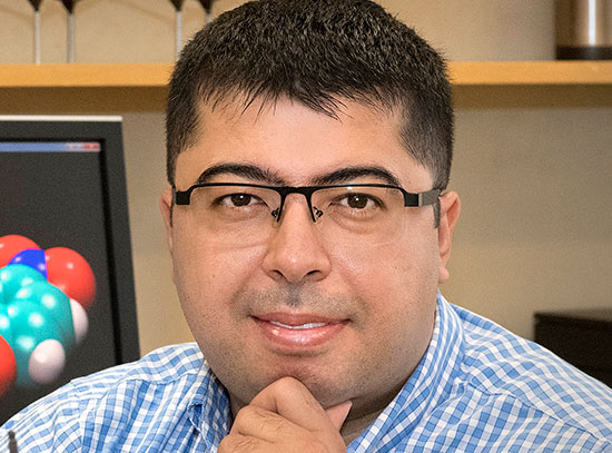
In 2017, Kjoller, who at the time worked for Anasys Instruments, and other Anasys scientists began engaging with the Center for Functional Nanomaterials (CFN)—a DOE Office of Science User Facility at Brookhaven National Laboratory—through a DOE Small Business Innovation Research (SBIR) award. The SBIR program, along with the related DOE Small Business Technology Transfer (STTR) program, encourages U.S. small businesses to engage in federal research and development with the potential for commercialization. The focus of Anasys was coupling two characterization techniques: infrared (IR) spectroscopy and scanning probe microscopy (SPM).
“Though SPM can measure the shape of a sample and lots of its properties such as electrical, magnetic, and thermal, it’s completely blind to chemical composition,” explained Kjoller. “Our goal was to couple IR spectroscopy, which can provide this chemical information via the photothermal effect, with a particular mode of SPM called atomic force microscopy.”
IR spectroscopy is based on how IR light interacts with molecular bonds in a sample, while AFM relies on a probe that scans over a sample surface and “feels” its topography. The photothermal effect occurs when a material absorbs and converts light energy into thermal energy (heat). By using AFM to measure the photothermal effect induced by the absorption of IR light, Anasys sought to address two questions commonly asked by researchers, particularly in the materials science and biological science communities: What is it, and where is it?
“AFM could provide a sense of where things were but you didn’t know what they were,” said Prater. “By adding IR spectroscopy, we could generate chemical maps to identify the different chemical species in a sample, and then determine the positions of these chemical species through AFM-IR imaging.”
Previously, scientists had to perform the two techniques separately. Correlating the measurements was difficult because the spatial resolution scales were very different—a few microns (millionths of a meter) for IR spectroscopy versus a few nanometers (billionths of a meter) for AFM. So, IR spectroscopy was not suited to do chemical analysis on the nanoscale.
“When we introduced our AFM-IR instrument, called nanoIR, in 2010, we made it possible for the first time to do broadly applicable chemical identification on the nanometer length scale,” said Kjoller.
One nanoIR instrument was installed in the CFN Proximal Probes Facility in 2018 and made available to CFN users. However, the initial instrument design did not incorporate environmental control. Typically, AFM-IR is performed in ambient pressure, meaning samples get exposed to water, oxygen, and other contaminants in the air; these contaminants can affect the reliability of the measurements, and temperature control is important to see how the structure and chemistry of materials evolve at elevated or reduced temperatures. At the CFN, staff scientist Samuel Tenney and group leader Dario Stacchiola of the Interface Science and Catalysis Group offered their expertise in performing experiments under controlled temperatures and pressures, from ultrahigh vacuum to reaction conditions. They customized an environmental cell with vacuum and variable-temperature control and incorporated it into the AFM-IR technology, leading to the manufacture of commercial AFM-IR instruments with this capability.
“With benchtop AFM, you can load samples by hand,” said Tenney. “But with a stainless-steel chamber around everything, you need an arm and adapters to transfer the samples. And this motion needs to be coupled with the moving mechanical probe on the AFM.
In 2018, Bruker acquired Anasys. That same year, Kjoller, Prater, and Anasys Chief Executive Officer Roshan Shetty co-founded Photothermal to develop another technology—optical photothermal IR spectroscopy, or O-PTIR—which combines IR spectroscopy with optical microscopy instead of AFM. Compared to AFMs, which require some level of expertise to operate and prepare samples for, optical microscopes are more intuitive.
Optical photothermal infrared (IR) spectroscopy—which combines IR spectroscopy with optical microscopy—enables IR imaging to chemically analyze samples (here, a bacterium) at a size scale smaller than one millionth of a meter.
“You simply put the sample inside the microscope and get an image,” explained Prater. “In addition, in many cases, such as for biological samples and fluids, scientists don’t need such high resolution. So, we identified an intermediate opportunity to enable chemical analysis without the complexity of an AFM. To give you a sense of how easy it can be, I recently taught someone who had never operated our instrument how to load his sample, collect the measurements, and perform the analysis. In about five minutes, he had identified the composition of his plastic.”
Tenney and Stacchiola are now helping in a similar capacity, leading the design of an environmental cell for one of Photothermal’s photothermal O-PTIR platforms: mIRage®. Because the O-PTIR technique is purely optical, no moving parts are required inside the cell, simplifying the engineering and allowing for more advanced environmental control. They are also modifying the instrument—dropping the sample stage to a lower height—to make sufficient space to accommodate the cell.
“The mIRage instrument with our new environmental cell will likely be available to CFN users later this year, enabling the study of nanomaterials in operando, or operating, conditions—one of the CFN strategic research themes,” said Tenney.
 enlarge
A mIRage-acquired image showing how the drug dexamethasone is distributed in a polymer matrix.
The mIRage instrument can collect both IR and Raman spectroscopy signals. While IR spectra are the result of vibrating molecules absorbing light, Raman spectra are the result of molecules inelastically scattering light, meaning energy is exchanged between light and matter. The O-PTIR technique uses a visible “probe beam” to measure IR absorption by the sample, and this same probe beam can be used to perform Raman spectroscopy. Thus, both IR and Raman spectra can be measured simultaneously at the same location with submicron spatial resolution. By collecting both signals at the same time and in the same location, mIRage provides complementary views of a sample’s chemistry. One example of where this capability is useful is modern drug formulations, which include active pharmaceutical ingredients that get released into the body over time and inactive ingredients like stabilizers and binders. The active ingredients provide a stronger Raman signal, whereas the inactive ingredients provide a stronger IR signal.
To develop the AFM-IR and O-PTIR technologies, Anasys and Photothermal received support not only from DOE SBIR and STTR programs but also several other complementary awards from government agencies, including the National Institutes of Standards and Technology, National Science Foundation, and National Institutes of Health. Kjoller and Prater attribute three primary factors key to their success: identifying opportunities in the marketplace, assembling a team with complementary skills, and understanding customer needs.
“We find gaps in the market, partner with innovators in the related fields to fill these gaps, and work with scientists on the technology development and application side to ensure they are successful in using them to solve compelling research problems,” said Prater.
“And we do so leveraging existing workflows,” added Kjoller. “For example, IR spectroscopy has been around for more than 40 years, so vast libraries of reference spectra are available on lots of materials. When we get spectra from our AFM-IR or O-PTIR instruments, we can correlate them with these material reference libraries to identify sample composition.”
Research institutes, universities, and companies around the world have been using both technologies for a range of applications—for example, to analyze failures during microelectronics manufacturing; investigate pathways for diseases such as Alzheimer’s and cancer; formulate polymer blends, multilayer films, coatings, and other materials; identify the components in historical paintings; and understand how ancient documents like vellum maps chemically degrade over time.
 enlarge
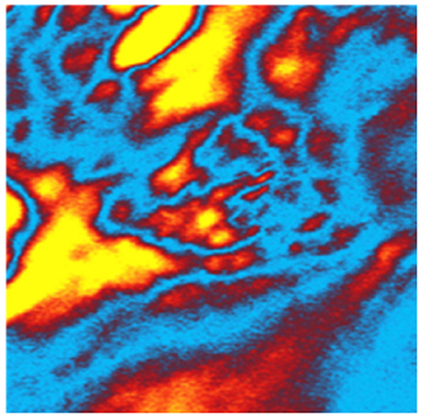
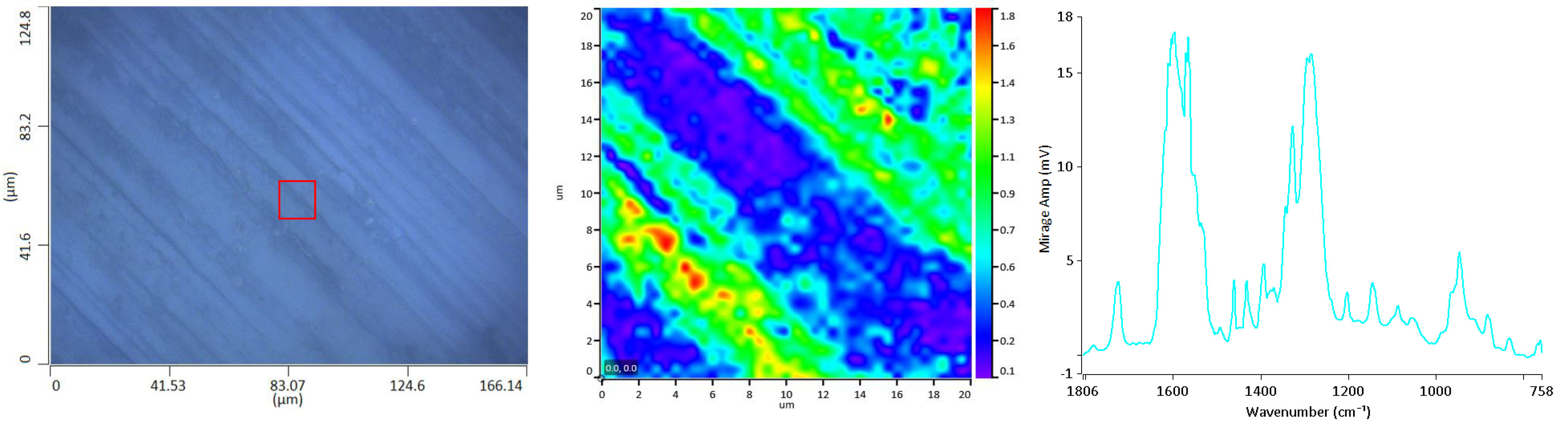
(Left) An optical image, taken at the CFN, of a sample containing pressure-sensitive organic material. (Middle) An O-PTIR chemical map from the defined region in the red box illustrating the chemical difference between regions exposed to higher pressure (red/yellow/green) and lower pressure (blue/purple) as a result of the manufacturing process. (Right) The corresponding O-PTIR spectra.
When the environmental cell–equipped mIRage with Raman instrument comes online at the CFN, it will support many research areas of interest to CFN staff and users, from structural biology and two-dimensional materials to energetics and catalysis.
“We’re trying to incorporate different environments for scientists to study liquid-solid interfaces, which would be useful for biological samples; gas-solid interfaces, which would be useful for catalysis; and extreme environments, which would be useful for energetics and superconductivity,” said Stacchiola.
The CFN team is also exploring ways to substantially increase the working pressure of the instrument. One example of where this high pressure may be relevant is for studies of room-temperature superconductivity, where electrons flow with zero resistance, without the expensive cooling to ultracold temperatures typically required.
Ultimately, the CFN team seeks to commercialize their environmental cell technology through the DOE STTR program.
Back at Photothermal, Kjoller and Prater also continue to add new capabilities. They recently released a newer version of their O-PTIR control and analysis software, which automates some of the tedious steps and simplifies the user interface.
“By further improving the user experience, we open up the technology to more users,” said Kjoller.
If you are a small business or startup interested in partnering with the CFN or a researcher interested in using the nanoIR or mIRage instruments at the CFN, contact CFN Assistant Director for Strategic Partnerships Priscilla Antunez at pantunez@bnl.gov.
Brookhaven National Laboratory is supported by the U.S. Department of Energy’s Office of Science. The Office of Science is the single largest supporter of basic research in the physical sciences in the United States and is working to address some of the most pressing challenges of our time. For more information, visit https://energy.gov/science.
Follow @BrookhavenLab on Twitter or find us on Facebook.
2021-19147 | INT/EXT | Newsroom