Valleytronics is Warming Up at Brookhaven Lab
CFN and Northrop Grumman researchers bring an innovative way to store and process information up to room temperature
September 8, 2023
 enlarge
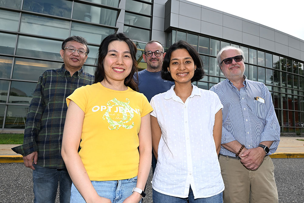
From left to right: Xiao Tong, Suji Park, Mircea Cotlet, Shreetu Shrestha, and Donald DiMarzio
UPTON, NY—Researchers at the Center for Functional Nanomaterials (CFN), a U.S. Department of Energy (DOE) Office of Science User Facility at DOE’s Brookhaven National Laboratory, and Northrop Grumman, a multinational aerospace and defense technology company, have found a way to maintain valley polarization at room temperature using novel materials and techniques. This discovery could lead to devices that store and process information in new ways using this technology without the need to keep them at ultra-low temperatures. Their research was recently published in Nature Communications.
One of the paths being explored to achieve these devices is a relatively recent field called “valleytronics”. A material’s electronic band structure—the range of energy levels in each atom’s electron configurations—can dip up or down. These troughs between the peaks are known as “valleys.” Some materials have multiple valleys with the same energy. An electron in a system like this can occupy any one of these valleys, presenting a unique way to store and process information based on which valley the electron occupies. One challenge, however, has been the energy and expense of maintaining the low temperatures needed to keep valley polarization stable. Without this stability, devices would begin to lose information. In order to make a technology like this feasible for practical, affordable applications, experts would need to find a way to around this constraint.
Exploring 2D Landscapes for the Perfect Valleys
Transition metal dichalcogenides (TMDs) are interesting, layered materials that can be, at their thinnest, only few atoms thick. Each layer in the material consists of a two-dimensional (2D) sheet of transition metal atoms sandwiched between chalcogen atoms. While the metal and the chalcogen are strongly bound by covalent bonds in a layer, adjacent layers are only weakly bound by van der Waal’s interactions. The weak bonds that hold these layers together enable TMDs to be exfoliated down to a monolayer that’s only one “molecule” thick. These are often referred to as 2D materials.
The team at CFN synthesized single crystals of chiral lead halide perovskites (R/S-NEAPbI3). Chirality describes a set of objects, like molecules, that are a mirror image of each other but can’t be superimposed. It is derived from the Greek word for “hands,” a perfect example of chirality. The two shapes are identical, but if you put one hand on top of the other, they will not align. This asymmetry is important for controlling valley polarization.
Flakes of this material, roughly 500 nanometers thick or five-thousandths the thickness of a human hair, were layered onto a monolayer of molybdenum disulfide (MoS2) TMD to create what is known as a heterostructure. By combining different 2D materials with properties that affect the charge transfer at the interface between the two materials, these heterostructures open up a world of possibility.
After creating and characterizing this heterostructure, the team was eager to see how it behaved.
A Degree of Freedom
“TMDs have two valleys with the same energy,” explained Shreetu Shrestha, a postdoctoral research associate at CFN and the author of this paper. “An electron can be in one valley or the other, which gives it an additional degree of freedom. Information can then be stored based on which valley an electron occupies.”
To get a better picture of the material’s behavior, the team leveraged tools at CFN’s Advanced Optical Spectroscopy and Microscopy facility. Scientists used a linearly polarized laser to excite the heterostructure they fabricated and then measured the light that was emitted from the molybdenum disulfide TMD using a confocal microscope. They performed the same process with a TMD that didn’t have the chiral lead halide perovskite layer added.
During these advanced experiments, the researchers noticed something interesting about the way light was emitted. The heterostructure had a lower emission than the bare TMD. The researchers attributed this behavior to the charge transferred from the TMD to the perovskite in the heterostructure. Using ultrafast spectroscopy, the researchers found that the charge transfers very quickly—only a few trillionths of a second.
The team also found that the intensity of the left and right circularly polarized components of the light emitted depends on the handedness of the chiral perovskite used. The chiral nature of the perovskite acted like a filter for electrons with different spin. Depending on the handedness of the chiral perovskite, electrons that spin either up or down were preferentially transferred from one valley over electrons with the opposite spin in the other valley. This phenomenon would enable researchers to selectively populate valleys and use their occupation in the same way current memory devices on computers store the 1s and 0s of binary bits.
“An important point to highlight in this experiment is that these results were realized at room temperature, which is where the whole field should move,” said Mircea Cotlet, a materials scientist at Brookhaven Lab and the principal investigator of the project. “Keeping hardware at the low temperatures that were being used is so much more complex and costly. It’s encouraging to see these kinds of material properties at room temperature.”
While valleytronics research is still at an early stage, researchers have already been thinking about possible applications. This technology could improve existing devices in surprising ways, expanding the capabilities of classical computers, but it could also be a component in the hardware of the future.
“This would help make classical computing more efficient,” said Shrestha, “but this technology could also be harnessed for quantum information science, which includes quantum computing, or even quantum sensing. These atomically thin materials have unique quantum properties, which we should be able to take advantage of.”
Fostering Collaboration and Innovation
CFN users and collaborators come from a wide range of fields in academia, research, and industry. This experiment involved contribution of a long-time collaborator from American global aerospace and defense technology company Northrop Grumman. In 2021, DOE’s Office of Energy Efficiency and Renewable Energy (EERE) awarded CFN with funding to collaborate with Northrop Grumman through the Technologist in Residence (TIR) program. The TIR program pairs senior technical staff from national labs and industry to conduct research and development. Programs like this strengthen national lab–industry relationships while advancing innovation in U.S. manufacturing and promoting economic growth and energy security.
“Our collaborations with Northrop Grumman and Don DiMarzio go back to 2015,” said Cotlet. “We have a mutual interest in 2D materials, particularly how they will help create the next generation of computers. It's encouraging to have the expertise of so many different people here under one roof. We are a user facility with access to a variety of high-end instruments and techniques which give us the ability to put all this information together.”
This work also allowed Shrestha and Cotlet to expand on the continued research that they have both been doing on TMDs and charge transfer.
“I had worked with perovskites during my PhD research and my first postdoctoral position,” said Shrestha, “so we were able to combine my expertise in that area with Mircea’s expertise in TMDs and the optical instruments we have in CFN’s Advanced Optical Spectroscopy and Microscopy facility to discover something promising. I was also excited to work with Suji Park and Xiao Tong of CFN and Mingxing Li, a scientist who was previously with CFN and is now at Innovare. This kind of understanding wouldn’t be possible without a collective effort and access to all of these high-end facilities under a single rooftop. I’m excited to see where this work leads and look forward to contributing more insight to CFN’s 2D materials program.”
Brookhaven National Laboratory is supported by the Office of Science of the U.S. Department of Energy. The Office of Science is the single largest supporter of basic research in the physical sciences in the United States and is working to address some of the most pressing challenges of our time. For more information, visit science.energy.gov.
Follow @BrookhavenLab on social media. Find us on Instagram, LinkedIn, Twitter, and Facebook.
2023-21376 | INT/EXT | Newsroom


