Small Size Enhances Charge Transfer in Quantum Dots
Single-particle study identifies possible path to improved conversion of sunlight to electricity in photovoltaic devices
December 16, 2013
 enlarge
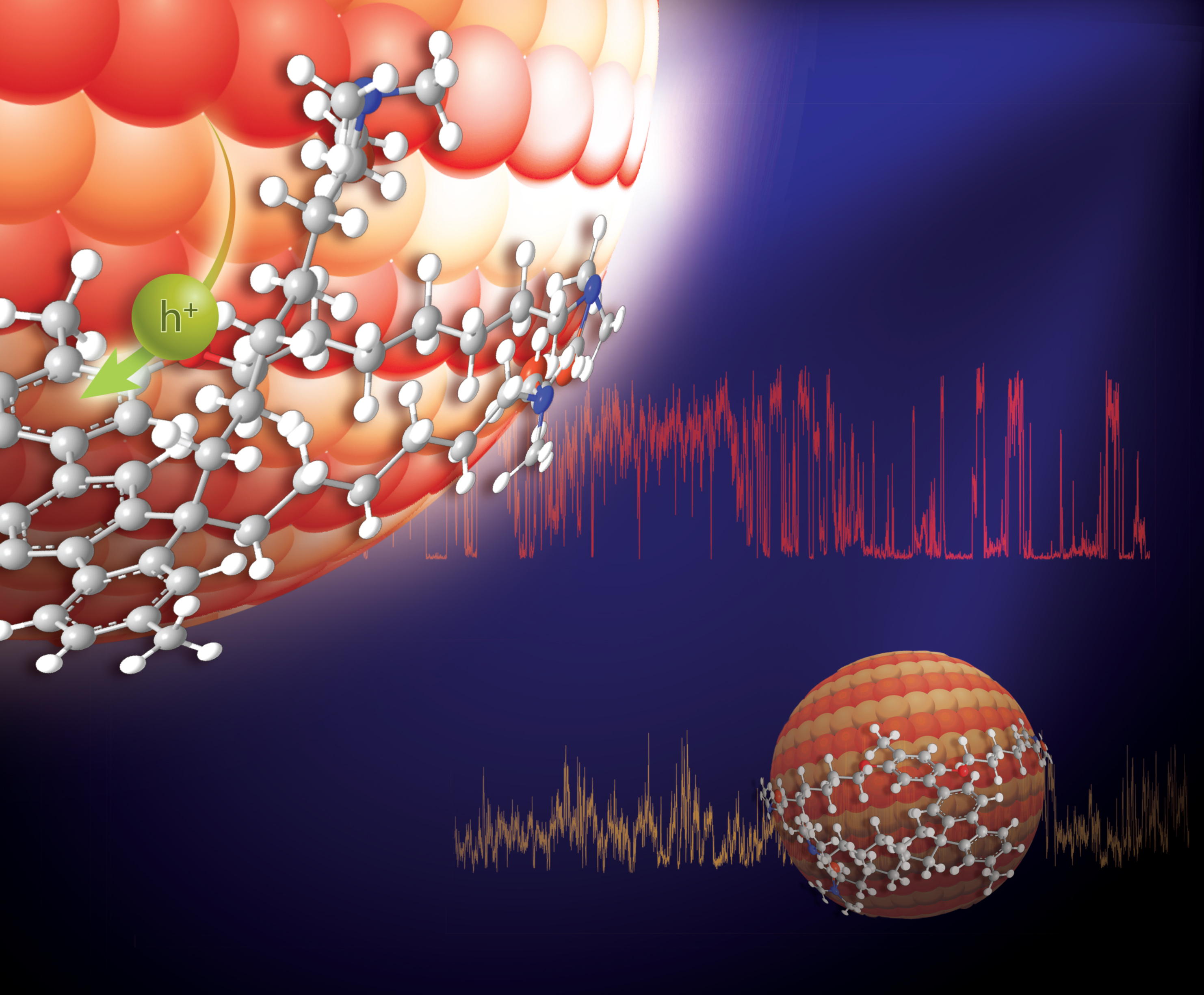
This illustration shows two light-absorbing quantum dots (orange/red spheres) surrounded by a conducting polymer ("stick-and-ball" structure). Shrinking the core of the quantum dot enhances the transfer of electric charges called "holes" (h+) from the quantum dot to the polymer. Quantum dots with enhanced charge transfer could find application in photovoltaic solar cells.
Quantum dots—tiny semiconductor crystals with diameters measured in billionths of a meter—have enormous potential for applications that make use of their ability to absorb or emit light and/or electric charges. Examples include more vividly colored light-emitting diodes (LEDs), photovoltaic solar cells, nanoscale transistors, and biosensors. But because these applications have differing—sometimes opposite—requirements, finding ways to control the dots’ optical and electronic properties is crucial to their success.
In a study just published in the journal Chemical Communications, scientists at the U.S. Department of Energy’s Brookhaven National Laboratory, Stony Brook University, and Syracuse University show that shrinking the core of a quantum dot can enhance the ability of a surrounding polymer to extract electric charges generated in the dot by the absorption of light.
“Photovoltaic cells made of quantum dots paired with plastic materials like conductive polymers are far easier to make and less expensive than conventional silicon-based solar cells,” said Mircea Cotlet, a physical chemist at Brookhaven’s Center for Functional Nanomaterials (CFN), who led the research team. “These kinds of materials are inexpensive, easy to synthesize, and their assembly would be relatively easy.”
The downside is that, right now, solar devices based on silicon can’t be beat in terms of efficiency. But research aimed at understanding the photovoltaic process at the nanoscale could change that.
“The ability to make and study single particles at the CFN allows us to observe and test properties that would be blurred, or averaged out, in larger samples,” said Huidong Zang, a postdoctoral research fellow working with Cotlet and first author on the paper.
In a solar cell, the ideal material would absorb a lot of light and efficiently convert that energy into electric charges that can be easily extracted as a current. To study the details of this process, the scientists used quantum dots composed of a light-absorbing cadmium-selenium core encased in a protective zinc-sulfide shell and surrounded by a conductive polymer. They tested the ability of the polymer to extract electric charges generated when the quantum dots absorbed light, and conducted experiments using quantum dots with cores of different sizes.
“We knew from theoretical predictions that particle size should have an effect on the charge transfer with the polymer, but no one had done this as an experiment until now, and in particular at the single-particle level,” Cotlet said.
When they varied the size of the quantum dot’s core, the scientists found that the smaller the diameter, the more efficient and more consistent the charge transfer process.
“By using a smaller core, we increased the efficiency of the charge transfer process and narrowed the distribution of the charge-transfer rate so it was closer to the ideal with less variability,” Zang said.
The scientists were exploring a particular type of charge transfer created by the movement of “holes”—areas of positive charge created by the absence of negatively charged electrons. In electronic devices, holes can be channeled just like electrons to create electric current. And in this case extracting holes had an added benefit—it increased the time that quantum dots, which turn on and off in a blinking pattern, remained in the “on” condition.
“Hole transfer inhibits blinking,” Cotlet said. “It keeps the quantum dot optically active longer, which is better for the photovoltaic process, because charges can only be extracted when the quantum dot is on.”
“It would be impossible to see this effect with bulk samples because you can’t see the ‘on’ and ‘off’ states. When lots of quantum dots are mixed together, the signals average out. You can only see it by looking at the single nanoparticles.”
 enlarge
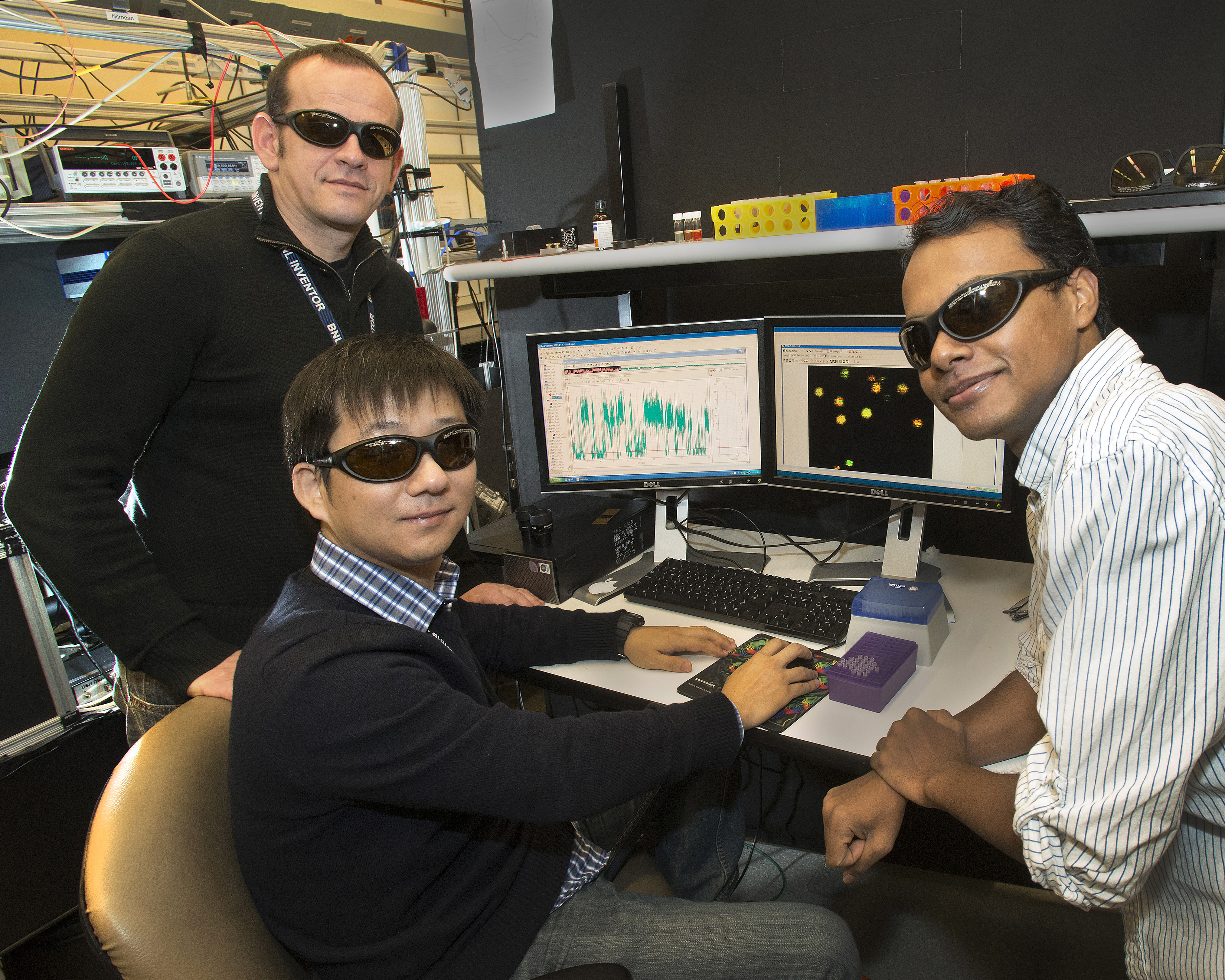
CFN's Mircea Cotlet (standing), post-doc Huidong Zang (center), and Prahlad Kumar Routh, a graduate student in the Materials Science Department at Stony Brook University, hope their research on quantum dots for solar cells will brighten our energy future. The scientists are wearing laser safety goggles required for their experiments.
Cotlet’s group had previously conducted a similar study pairing quantum dots with carbon-rich buckyballs. In that study, they found the opposite effect: Buckyballs decreased the dots “on” time while enhancing the transfer of electrons.
In other applications combing dots and polymers, such as LEDs or biosensors, scientists are looking for ways to suppress charge transfer as this process becomes detrimental.
“Knowing these fundamentals and how to control these processes at the nanoscale should help us optimize the use of quantum dots for a wide range of applications,” Cotlet said.
This research was funded by the DOE Office of Science and by the Air Force Office of Scientific Research.
DOE’s Office of Science is the single largest supporter of basic research in the physical sciences in the United States, and is working to address some of the most pressing challenges of our time. For more information, please visit science.energy.gov.
The Center for Functional Nanomaterials at Brookhaven National Laboratory is one of the five DOE Nanoscale Science Research Centers (NSRCs), premier national user facilities for interdisciplinary research at the nanoscale. Together the NSRCs comprise a suite of complementary facilities that provide researchers with state-of-the-art capabilities to fabricate, process, characterize and model nanoscale materials, and constitute the largest infrastructure investment of the National Nanotechnology Initiative. The NSRCs are located at DOE’s Argonne, Brookhaven, Lawrence Berkeley, Oak Ridge and Sandia and Los Alamos national laboratories. For more information about the DOE NSRCs, please visit http://nano.energy.gov.
2013-4487 | INT/EXT | Newsroom


