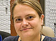
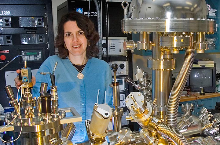
10 Questions with Eli Sutter
interview with a CFN Scientist
April 6, 2013
Understanding the intricacies—both internal and external—of nanoscale materials and processes can drive innovations that push the technology found inside everything from electric vehicles to smart phones. Advancing such crucial high-tech building blocks requires detailed portraits of the nanoworld, and that's where the expertise of physicist Eli Sutter is essential. Sutter, who works at Brookhaven Lab's Center for Functional Nanomaterials (CFN), is uniquely skilled at revealing tiny materials that carry tremendous potential.
What is your research specialty at the Center for Functional Nanomaterials?
I am a scientist at the electron microscopy facility, and my particular focus is on transmission electron microscopy (TEM) of nanomaterials. The TEM operates on the same principle as a light microscope, only it uses a beam of electrons instead of light. The resolution of the best light microscopes is limited by visible light's wavelength to about 200 nanometers. The electrons used in a TEM, however, have wavelengths as small as 0.0025 nanometers (for 200 kV electrons), and the resolution limits actually come from aberrations in the lenses. Nevertheless a much better resolution is achieved in TEM—currently individual atomic columns. The electrons interact with the sample and are transmitted through it, and as a result a magnified image of the sample is formed on a fluorescent screen, camera, or detector. Apart from images, the interactions of the electrons with the sample provide all kinds of information about it: crystal structure and morphology, chemical composition, electronic structure, and magnetic domains, among others.
What sorts of experiments are ideally suited for TEM studies?
I perform a variety of experiments, from imaging and chemical characterization of thin films and nanostructures to real-time time studies of nanoscale processes. One group of experiments includes in-situ variable temperature TEM experiments—studying the way materials transform when the temperature changes. This work gives insight into alloy phase diagrams, solute solubility, phase transformations, oxidation, and solid-state reactions.
Are there any recent developments in TEM that you apply at CFN?
Yes, actually. I perform TEM in liquid environments, which is exciting because TEM imaging is traditionally done in high vacuum conditions. This capability was only developed very recently, and we are just now starting to "look" in real time at processes in liquids and solutions. This work aims at understanding organization of nanoparticles in colloids and solutions, growth processes, electro-deposition, and more.
What kinds of nanomaterials or thin films do you work with, and what makes those materials interesting or impactful?
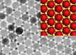
I work with a wide range of materials: metallic nanoparticles, semiconductor nanowires, core-shell nanoparticles and nanowires, and two-dimensional materials such as graphene. All these nanomaterials are of interest because they find applications in catalysts, sensors, fuel cells, batteries, medical imaging, targeted drug delivery, and other technologies. We always face the challenge of improving their structure and properties, as well as designing entirely new materials, and this stimulates and advances basic scientific research.
How did you first get involved with physics and materials science?
I was really interested in physics at school, and I decided to pursue that field all the way through my Ph.D. in Condensed Matter Physics at Sofia University "St. Kliment Ohridsi"—the oldest, largest, and most prestigious university in Bulgaria. Even now, my research remains as stimulating and exciting to me as ever.
What questions about energy, technology, or fundamental science do you address?
When I pick a project, I always try to address large challenges or question long-held conventional wisdom. For example, an existing theory held that the transformation of liquid drops into solid particles began by formation of a crystalline grain in the interior of the drop, but we found that in nanoscale droplets the crystallization begins at their surfaces. This took some tremendous experimental precision, including dispensing liquid droplets of a gold-germanium alloy with zeptoliter volumes—just billionths of a trillionth of a liter—inside the TEM and observing their behavior while changing the temperature.
What attracts you to a new experiment or potential collaboration with CFN users or staff scientists?
The experiments that I find particularly attractive are the ones designed to understand phenomena on the nanoscale, such as how nanomaterial processes can differ from those occurring in the identical materials in a bulk form. Scale can make a world of difference in materials science. Experiments that reveal these processes in real-time can directly identify pathways to functional nanomaterials.
What is one experiment or collaborations in which you're currently involved?
As I mentioned briefly before, I work with semiconductor nanowires that are formed by vapor-liquid-solid (VLS) growth. Central to the VLS process is a liquid metal-semiconductor alloy seed drop whose equilibrium with the adjacent nanowire governs all aspects of the growth process. Given the small size of the alloy drop—typically a few tens of nanometers—the known phase diagrams for the bulk materials cannot provide a reliable basis for predicting growth phenomena. So we have developed real-time microscopy techniques to establish the nanoscale phase diagrams of the drops used in VLS nanowire growth.
This knowledge enhances the ability to predict nanowire growth, which suffers from extreme sensitivity to multiple parameters. Our findings demonstrated general avenues for synthesizing nanowire heterostructures involving controlled morphologies, pathways to doping, and access to metastable solid phases—and this is all applicable to the wide range of materials for which nanowires are grown by the VLS method.
What's one way in which CFN users benefit from other facilities and opportunities at Brookhaven Lab?
The synergy with the National Synchrotron Light Source (NSLS) is a major component of the work at CFN. Users can even submit proposals for combined research to both facilities simultaneously, and it can often be arranged so that scientists get access to CFN facilities for sample preparation and concurrently for measurements at NSLS during the same visit. I expect that cross-facility work to become even more innovative after NSLS-II begins operations in 2014.
Why should users come to CFN to do their research?
CFN provides state-of-the-art equipment that is not just a collection of different high-end instruments, but also a well thought-out selection that allows for a plethora of characterizations on a large spectrum of materials to be performed under the same roof. The CFN is also a place where scientists and professional experts are available and ready to discuss new challenges and provide advice and solutions to users. This very powerful combination drives success in any scientific endeavor.
2013-3876 | INT/EXT | Newsroom