Enhancing Materials for Hi-Res Patterning to Advance Microelectronics
Scientists at Brookhaven Lab's Center for Functional Nanomaterials created "hybrid" organic-inorganic materials for transferring ultrasmall, high-aspect-ratio features into silicon for next-generation electronic devices
August 27, 2019
 enlarge
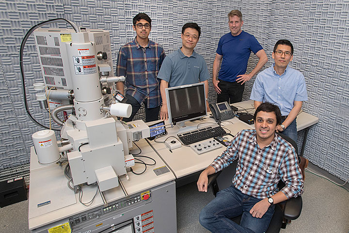
(Left to right): Ashwanth Subramanian, Ming Lu, Kim Kisslinger, Chang-Yong Nam, and Nikhil Tiwale in the Electron Microscopy Facility at Brookhaven Lab's Center for Functional Nanomaterials. The scientists used scanning electron microscopes to image high-resolution, high-aspect-ratio silicon nanostructures they etched using a "hybrid" organic-inorganic resist.
UPTON, NY—To increase the processing speed and reduce the power consumption of electronic devices, the microelectronics industry continues to push for smaller and smaller feature sizes. Transistors in today’s cell phones are typically 10 nanometers (nm) across—equivalent to about 50 silicon atoms wide—or smaller. Scaling transistors down below these dimensions with higher accuracy requires advanced materials for lithography—the primary technique for printing electrical circuit elements on silicon wafers to manufacture electronic chips. One challenge is developing robust “resists,” or materials that are used as templates for transferring circuit patterns into device-useful substrates such as silicon.
Now, scientists from the Center for Functional Nanomaterials (CFN)—a U.S. Department of Energy (DOE) Office of Science User Facility at Brookhaven National Laboratory—have used the recently developed technique of infiltration synthesis to create resists that combine the organic polymer poly(methyl methacrylate), or PMMA, with inorganic aluminum oxide. Owing to its low cost and high resolution, PMMA is the most widely used resist in electron-beam lithography (EBL), a kind of lithography in which electrons are used to create the pattern template. However, at the resist thicknesses that are necessary to generate the ultrasmall feature sizes, the patterns typically start to degrade when they are etched into silicon, failing to produce the required high aspect ratio (height to width).
As reported in a paper published online on July 8 in the Journal of Materials Chemistry C, these “hybrid” organic-inorganic resists exhibit a high lithographic contrast and enable the patterning of high-resolution silicon nanostructures with a high aspect ratio. By changing the amount of aluminum oxide (or a different inorganic element) infiltrated into PMMA, the scientists can tune these parameters for particular applications. For example, next-generation memory devices such as flash drives will be based on a three-dimensional stacking structure to increase memory density, so an extremely high aspect ratio is desirable; on the other hand, a very high resolution is the most important characteristic for future processor chips.
“Instead of taking an entirely new synthesis route, we used an existing resist, an inexpensive metal oxide, and common equipment found in almost every nanofabrication facility,” said first author Nikhil Tiwale, a postdoctoral research associate in the CFN Electronic Nanomaterials Group.
Though other hybrid resists have been proposed, most of them require high electron doses (intensities), involve complex chemical synthesis methods, or have expensive proprietary compositions. Thus, these resists are not optimal for the high-rate, high-volume manufacture of next-generation electronics.
Advanced nanolithography for high-volume manufacturing
Conventionally, the microelectronics industry has relied upon optical lithography, whose resolution is limited by the wavelength of light that the resist gets exposed to. However, EBL and other nanolithography techniques such as extreme ultraviolet lithography (EUVL) can push this limit because of the very small wavelength of electrons and high-energy ultraviolet light. The main difference between the two techniques is the exposure process.
“In EBL, you need to write all of the area you need to expose line by line, kind of like making a sketch with a pencil,” said Tiwale. “By contrast, in EUVL, you can expose the whole area in one shot, akin to taking a photograph. From this point of view, EBL is great for research purposes, and EUVL is better suited for high-volume manufacturing. We believe that the approach we demonstrated for EBL can be directly applied to EUVL, which companies including Samsung have recently started using to develop manufacturing processes for their 7 nm technology node.”
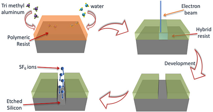
In this study, the scientists used an atomic layer deposition (ALD) system—a standard piece of nanofabrication equipment for depositing ultrathin films on surfaces—to combine PMMA and aluminum oxide. After placing a substrate coated with a thin film of PMMA into the ALD reaction chamber, they introduced a vapor of an aluminum precursor that diffused through tiny molecular pores inside the PMMA matrix to bind with the chemical species inside the polymer chains. Then, they introduced another precursor (such as water) that reacted with the first precursor to form aluminum oxide inside the PMMA matrix. These steps together constitute one processing cycle.
 enlarge
A schematic showing the process of creating the hybrid organic-inorganic resist through infiltration synthesis, patterning the resist via electron-beam lithography, and etching the pattern into silicon by bombarding the silicon surface with ions of sulfur hexafluoride (SF6).
The team then performed EBL with hybrid resists that had up to eight processing cycles. To characterize the contrast of the resists under different electron doses, the scientists measured the change in resist thickness within the exposed areas. Surface height maps generated with an atomic force microscope (a microscope with an atomically sharp tip for tracking the topography of a surface) and optical measurements obtained through ellipsometry (a technique for determining film thickness based on the change in the polarization of light reflected from a surface) revealed that the thickness changes gradually with a low number of processing cycles but rapidly with additional cycles—i.e., a higher aluminum oxide content.
“The contrast refers to how fast the resist changes after being exposed to the electron beam,” explained Chang-Yong Nam, a materials scientist in the CFN Electronic Nanomaterials Group, who supervised the project and conceived the idea in collaboration with Jiyoung Kim, a professor in the Department of Materials Science and Engineering at the University of Texas at Dallas. “The abrupt change in the height of the exposed regions suggests an increase in the resist contrast for higher numbers of infiltration cycles—almost six times higher than that of the original PMMA resist.”
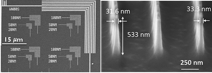
The scientists also used the hybrid resists to pattern periodic straight lines and “elbows” (intersecting lines) in silicon substrates, and compared the etch rate of the resists with substrates.
 enlarge
Left: A scanning electron microscope (SEM) image of silicon elbow-shaped nanopatterns with different feature sizes (linewidths). Right: A high-magnification SEM image of high-resolution, high-aspect-ratio silicon nanostructures patterned at a pitch resolution (linewidth plus spacewidth, or space between lines) of 500 nm.
“You want silicon to be etched faster than the resist; otherwise the resist starts to degrade,” said Nam. “We found that the etch selectivity of our hybrid resist is higher than that of costly proprietary resists (e.g., ZEP) and techniques that use an intermediate “hard” mask layer such as silicon dioxide to prevent pattern degradation, but which require additional processing steps.”
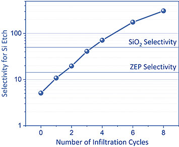 enlarge
After two processing cycles, the etch selectivity of the hybrid resist surpasses that of ZEP, a costly resist. After four cycles, the hybrid resist has a 40 percent higher etch selectivity than that of silicon dioxide (SiO2).
Going forward, the team will study how the hybrid resists respond to EUV exposure. They have already started using soft x-rays (energy range corresponding to the wavelength of EUV light) at Brookhaven’s National Synchrotron Light Source II (NSLS-II), and hope to use a dedicated EUV beamline operated by the Center for X-ray Optics at Lawrence Berkeley National Lab’s Advanced Light Source (ALS) in collaboration with industry partners.
“The energy absorption by the organic layer of EUVL resists is very weak,” said Nam. “Adding inorganic elements, such as tin or zirconium, can make them more sensitive to EUV light. We look forward to exploring how our approach can address the resist performance requirements of EUVL.”
Both NSLS-II and ALS are DOE Office of Science User Facilities. The other co-authors are CFN scientists Kim Kisslinger, Ming Lu, and Aaron Stein; and Ashwanth Subramanian, a PhD student in the Department of Materials Science and Chemical Engineering at Stony Brook University and a graduate research assistant at the CFN.
Brookhaven National Laboratory is supported by the U.S. Department of Energy’s Office of Science. The Office of Science is the single largest supporter of basic research in the physical sciences in the United States and is working to address some of the most pressing challenges of our time. For more information, visit https://energy.gov/science.
Follow @BrookhavenLab on Twitter or find us on Facebook.
2019-16681 | INT/EXT | Newsroom


