- Home
- Facilities
- Research
-
Working at CFN
- Arrival & Departure
- Reports & Publications
- Acknowledging Use of CFN Facilities
- Data Management
- The Guide to Brookhaven
Safety Procedures
- Operations Plan
- Experimental Safety Reviews (ESR)
- COSA Training
- Hours of Operation
- Laser System Qualification
- Transport of Hazardous Materials
- Vendor On-site Scheduling Procedure (PDF)
- Electrical Equipment Inspections
- News & Events
- People
- Jobs
- Contact
- Business
- Intranet
Hitachi HD2700C Scanning Transmission Electron Microscope
Contacts: Sooyeon Hwang | Lihua Zhang
The Hitachi 2700C is a dedicated Scanning Transmission Electron Microscope (STEM), operating at 80, 120 and 200 kV. It has a probe aberration-corrector, which improves imaging spatial resolution to less than 1Å. The energy resolution for electron energy loss spectroscopy (EELS) can be as small as 0.35 eV, due to its cold field emission electron gun (FEG) and the presence of a high-resolution parallel EELS detector (Gatan Enfina-ER). This instrument is ideal for probing structural and electronic properties of materials at the Angstrom level, allowing on to study the physical, chemical and electronic structure of oxide interfaces, catalysts and other functional nanomaterials. Notably, this Hitachi STEM has a secondary electron microscopy (SEM) detector for high resolution SEM imaging of the particles on the surface, with atomic resolution imaging have been demonstrated in the SEM imaging mode.
Specifications
- Accelerating voltage: 80~200 kV
- Spherical aberration (C3): <1um
- Chromatic aberration: 0.75 mm
- Operating vacuum (specimen): ~10e-6 Pa
- Cold FEG
Detectors
- High-Angle Annular Dark Field
- Medium-Angle Annular Dark Field
- Bright Field
- Secondary Electron Detector
- Diffraction Cameras
- Gatan Enfinium EELS spectrometer
- Bruker SDD EDX detector (to be installed in Nov 2010)
Resolution
- Imaging: ~0.9 Å
- Energy resolution: ~0.35 eV
- SEM imaging: ~1.4 Å
References
(1) H. Inada, L. Wu, J. Wall, D. Su, and Y. Zhu, J. Electron Microscopy, 58 (2009) 111
(2) Y. Zhu, H. Inada, K. Nakamura, and J. Wall, Nature Materials, 8 (2009) 808
Example Images & Spectra
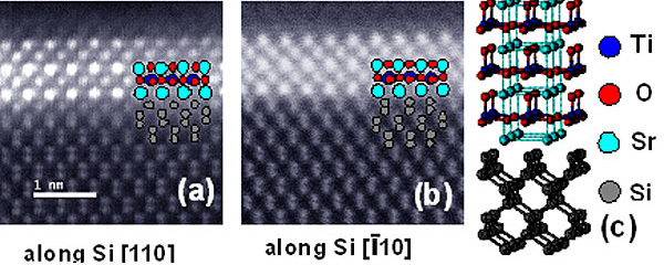
High-angle annular dark field imaging: (a) and (b) High angle annular dark field (HAADF) images on SrTiO3/Si interface. (c) The structure model from a b initio calculation confirmed the atomic structure at the interface showing in (a) and (b).
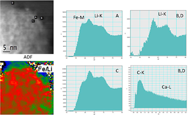
EELS at high spatial resolution: EELS is a powerful technique to probe the local compositional and electronic information. Here is an example of EELS-2D mapping on Li-battery electrode materials as how Li and Fe elements distributed at nanometer scale.
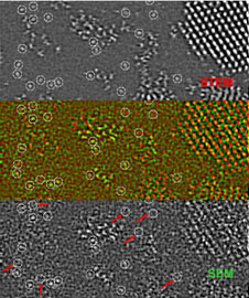
SEM Imaging. The recent achievement of 0.1nm in atomic imaging using the Hitachi HD2700C STEM suggests that SE imaging can now achieve comparable spatial resolution to the STEM mode but with complementary capabilities. For instance, as shown below, simultaneous acquisition of the SE image using secondary electrons (bottom) and the ADF-STEM image using transmitted electrons (top) of uranium oxide nanocrystals and uranium individual atoms (filtered with unsharp mask in real space) on a 2-nm carbon support.