Synthesis Method Expands Material Possibilities
Scientists are making functional inorganic and "hybrid" materials—those containing both inorganic and organic components—with tunable properties for a wide range of applications, including microelectronics, sensing, and clean energy
April 23, 2021
 enlarge
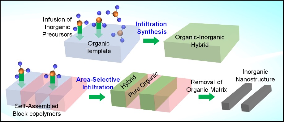
Schematics describing the infiltration synthesis process for making new materials. Top: Generation of an organic-inorganic hybrid by infiltrating inorganic precursors (starting materials) into an organic template, such as a polymer thin film. Bottom: Area-selective infiltration into block copolymers, or polymers self-assembled from two or more chemically distinct "blocks." The inorganic precursor is only infiltrated in blue polymer domains. The organic matrix is then selectively removed to generate inorganic nanostructures inheriting the geometry of the starting polymer domain.
Since the beginning of civilization, humans have exploited new materials to improve their lives, from the prehistoric Stone Age, Bronze Age, and Iron Age to the modern Silicon Age. With each period came technological breakthroughs that transformed the way we live. Consider the 1961 invention of the silicon chip, which paved the way for the digital revolution. Without this tiny electronic component, we’d have no laptops or cell phones.
 enlarge
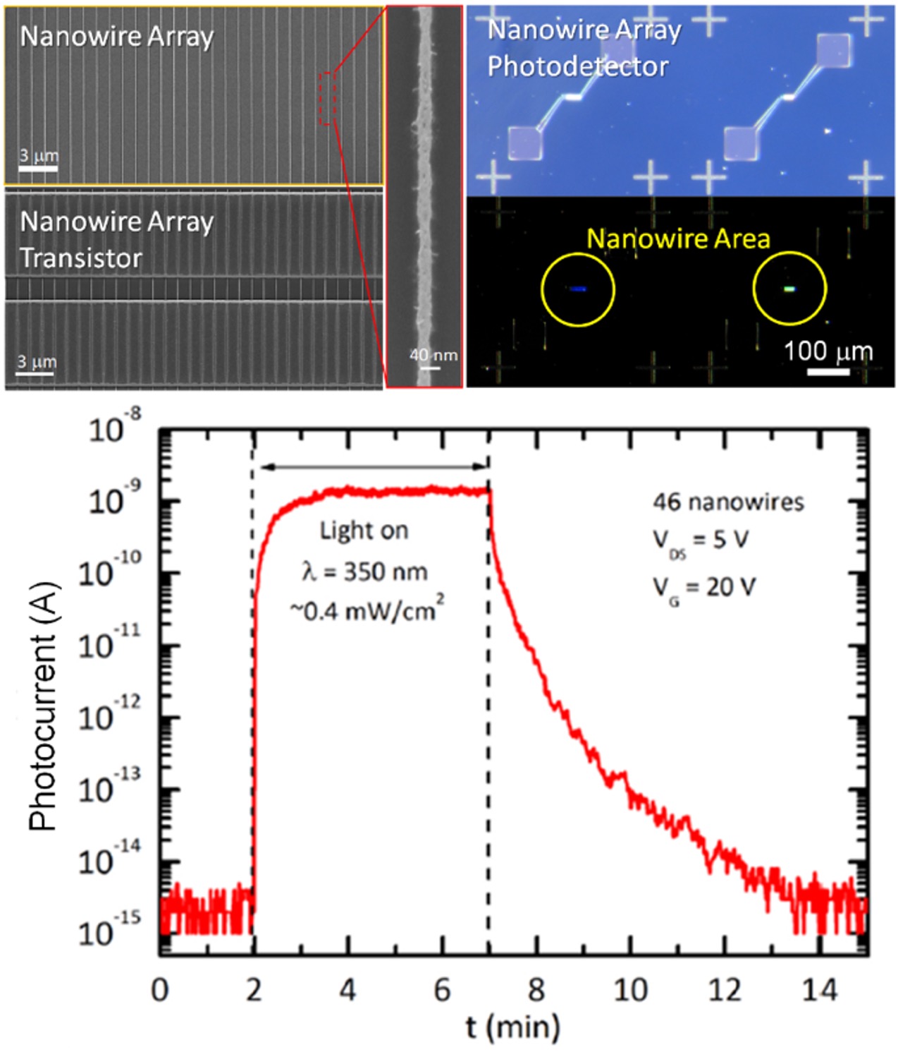
Scanning electron and optical microscope images of a zinc oxide nanowire array, nanowire array transistor, and nanowire array photodetector of ultraviolet (UV) light (top). The scientists combined infiltration synthesis and lithography to fabricate precisely aligned nanowire arrays and integrate them into devices. The photodetector has ultrahigh sensitivity to UV light, as shown in the graph (bottom). Research published in Advanced Optical Materials (2017).
Addressing today’s challenges will similarly require material advances. For example, how do we make solar panels that convert sunlight into electricity more efficiently? Batteries that last longer? Ever-smaller electronic devices? Scientists are seeking solutions to these very questions through materials science and engineering. They’re both improving the performance of existing materials and creating brand-new materials with unparalleled properties.
Over the past decade, scientists at the Center for Functional Nanomaterials (CFN) at the U.S. Department of Energy (DOE)’s Brookhaven National Laboratory have established themselves as leaders in this area. In particular, they are developing a new method for making materials: infiltration synthesis.
As its name suggests, infiltration synthesis involves infiltrating, or infusing, one material into another. By infusing an inorganic (non-carbon-containing) material in an organic (carbon-containing) material, one can generate a “hybrid” material with properties not seen in either of the starting components. The organic species could be polymer thin films, polymers patterned in a particular geometrical shape using a light source or electron beam (a technique known as lithography), polymers self-assembled from two or more chemically distinct “blocks” (block copolymer), or even self-assembled DNA structures. Infiltration occurs as the organic matrix is exposed to inorganic-containing gas or liquid precursors (starting materials) in an alternating order.

By placing the hybrid material under oxygen plasma (an electrically charged gas) or in a high-temperature oxygen environment, scientists can also selectively remove the organic component. The inorganic part remains behind and inherits the organic “template” pattern, which is useful for creating inorganic nanostructures and integrating them into electronic devices.
“Conventional pure chemistry-based approaches like chemical synthesis are complex,” explained Chang-Yong Nam, a scientist in the CFN Electronic Nanomaterials Group who is leading the infiltration synthesis research. “There’s no guarantee you’ll end up with the properties you targeted. And creating very small features—which are important for making electronic devices—is difficult. Infiltration synthesis addresses these issues, and the required tools are readily available in any nanofabrication facility.”
Nam, CFN colleagues, and external collaborators have been demonstrating how infiltration synthesis can be used to create a host of new functional materials, enabling a wide variety of applications.
 enlarge
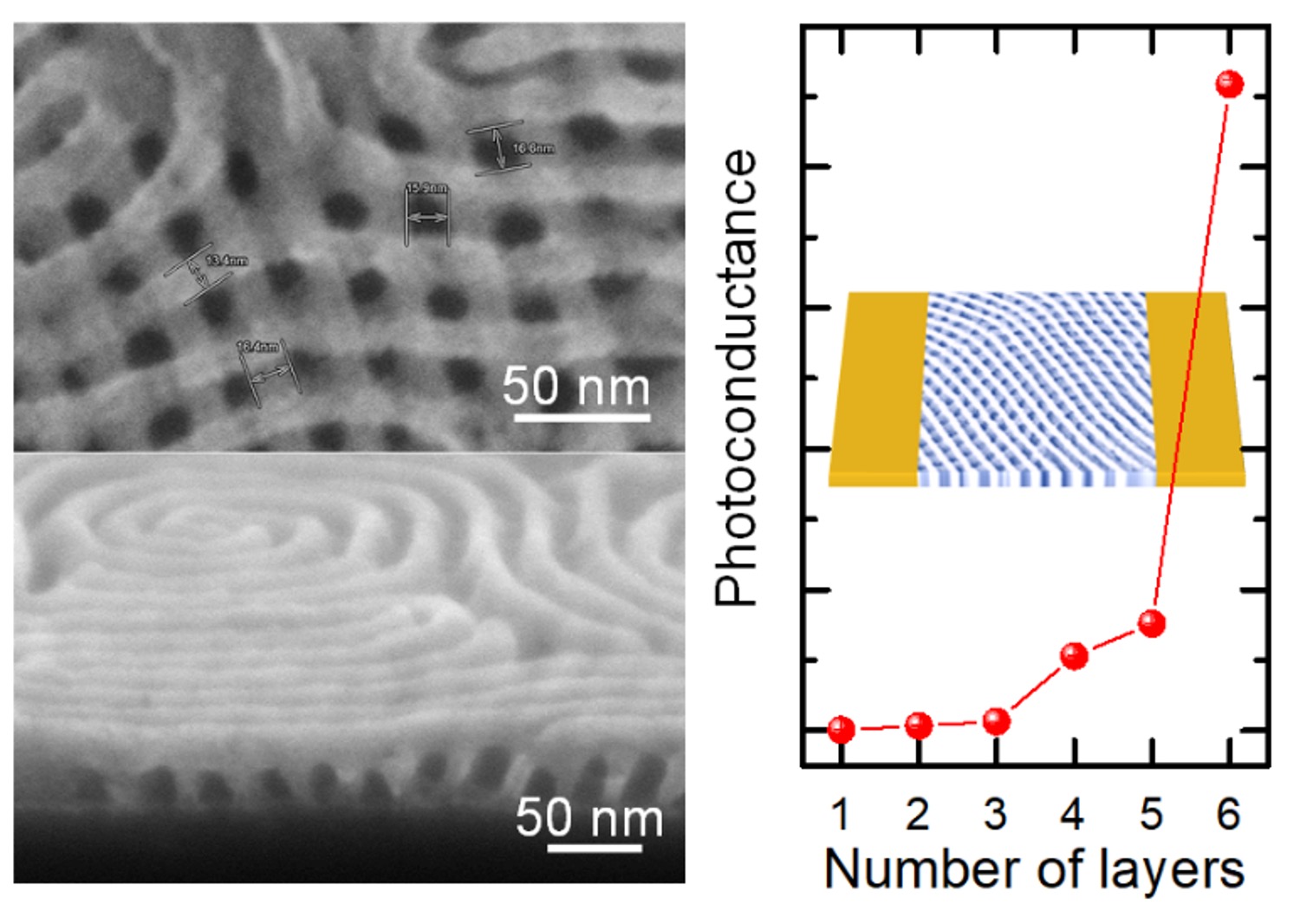
(Left) Top- and side-view scanning electron microscope images of a ZnO nanomesh. (Right) A nanomesh device with electrodes (yellow) patterned by lithography. As shown in the graph, the device with six layers absorbed the most ultraviolet light, leading to the highest electrical currents. Research published in Nanoscale (2019).
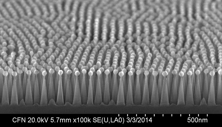
In 2015, they used infiltration synthesis and lithography to pattern inorganic nanowires—wire-shaped structures with a width on the order of billionths of a meter—into a transistor. This study was the first to show that the technique could be used to pattern an electronic device. Extending this initial concept, they made arrays of perfectly aligned nanowires into highly sensitive photodetectors of ultraviolet (UV) light. To increase sensitivity even further, they converted stacked self-assembling block copolymer patterns into a 3-D “nanomesh” architecture. The large surface area and pores enabled by this 3-D layered geometry allowed for the placement of many more nanowire sensing elements.
This combination of block copolymer self-assembly and infiltration synthesis has also enabled various innovations by other research teams at the CFN. For example, one team used the technique to texture the surface of silicon solar cells with cone-shaped nanostructures. Similar tiny structures cover moth eyes to prevent light reflection, and the scientists demonstrated this antireflective effect in the nanotextured solar cells, as well as on “invisible glass” surfaces. When light strikes a solar cell, you want to minimize reflection (or alternatively, maximize absorption) so that the solar energy can be efficiently converted into electricity. And for display screens on computers, cell phones, and other electronics, you want to eliminate light reflection to prevent glare.
 enlarge
A scanning electron microscope image of the antireflective "nanocones." Research published in Nature Communications (2015).
Following these studies on inorganic materials, the scientists began exploring the properties of hybrid organic-inorganic materials also generated by infiltration synthesis. For example, they created hybrid “nanopillars” exhibiting both the high strength of a metal and the low stiffness of foam. With this rare combination of mechanical properties, the material can store and release an unprecedented amount of elastic energy, making it useful for devices requiring ultrasmall springs, levers, or motors—such as accelerometers, resonators, and biosynthetic artificial muscles.
The scientists also showed how hybrids can serve as optical coatings that reflect specific wavelengths of light; highly sensitive oxygen and water sensors; photoresists for transferring ultrasmall features into silicon for next-generation microelectronics; all-around coatings on individual nanoparticles for cell tagging and tracking in biological imaging; and contrast agents to visualize the complex geometry of 3-D block copolymers.
 enlarge
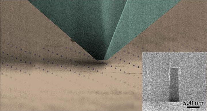
A scanning electron microscope image of a nanomechanical testing tip passing over arrays of the hybrid nanopillars. The tip gently applies pressure to test the elasticity and energy storage potential of the structures. The structure of an individual nanopillar—about 200 times thinner than a human hair—is shown in the inset. Research published in Nano Letters (2017).
“The amazing thing about infiltration synthesis is the tunability,” said Kevin Yager, leader of the CFN Electronic Nanomaterials Group. “You can very precisely dial-in desired material properties by selecting the right infiltrant and the right loading level. This lets you target a huge variety of applications and optimize the material for each specific task.”
More recently, the scientists have been studying the suitability of their hybrid resists for extreme UV (EUV) lithography. Semiconductor technology companies are using this emerging technique to shrink transistors—the building blocks of electronic components like central processing units (CPUs) and random-access memory (RAM)—down below five nanometers. Reducing feature dimensions will enable the fabrication of electronic devices with increased processing speeds and lower power consumption. Despite the promise of EUV lithography, several challenges remain, including the need for high-sensitivity resists.
 enlarge
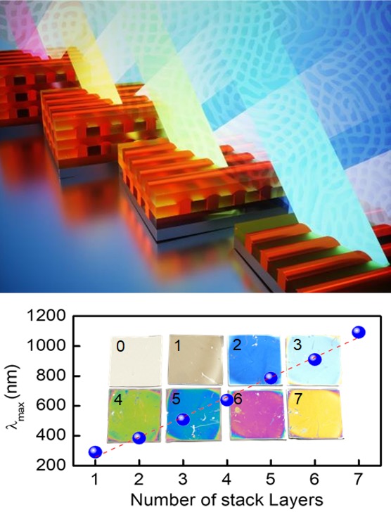
(Top) Illustration of stacked self-assembled block copolymer thin films that have been infiltrated with platinum (Pt). The colored background image shows a Pt nanomesh obtained by removing the organic matrix; the nanomesh could be used in catalysis and chemical sensing. (Bottom) The hybrid thin films change color depending on the number of stacked layers. Research published in ACS Applied Material Interfaces (2020).
“EUV lithography requires resists that can absorb a high amount of EUV light, and organic materials typically lack this capacity,” explained Nam. “Infiltrating an inorganic species into the organic component can improve absorptivity.”
Though many groups are now developing resist technologies, a fundamental-level understanding of the infiltration chemistry and EUV exposure process in resists is lacking. Nam and his team have started studying this mechanism in their hybrid resists through electron-beam lithography and low-energy electron microscopy at the CFN and x-ray scattering and absorption spectroscopy at the Soft Matter Interfaces (SMI) and Spectroscopy Soft and Tender (STT) beamlines of Brookhaven’s National Synchrotron Light Source II. They are also exploring the EUV exposure characteristics and patterning performance of the hybrid resists at the Microfield Exposure Tool (MET) beamline—a private EUV beamline sponsored by leading semiconductor companies, including Intel Corporation and Samsung Electronics—of Lawrence Berkeley National Lab’s Advanced Light Source. Their preliminary results provided important feedback on how to optimize the infiltration chemistry and method for enhanced EUV sensitivity.
 enlarge
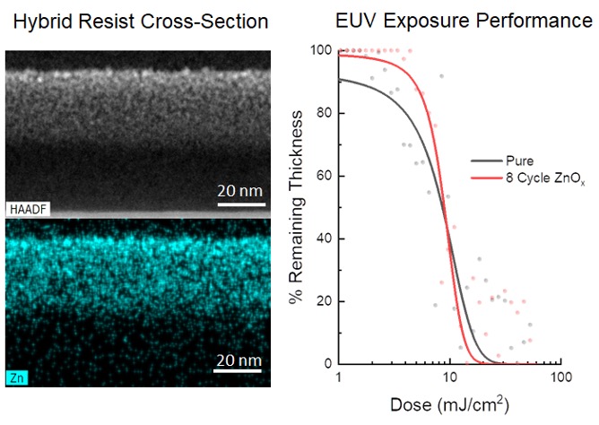
(Left) Transmission electron microscope images of cross-sections of a ZnO-infiltrated hybrid resist. (Right) Extreme ultraviolet (EUV) exposure performance of the hybrid resist and an uninfiltrated polymer. ZnO infiltration enhances EUV sensitivity (decreased critical dose) and exposure contrast (increased slope of curve). Research published in SPIE Proceedings (2021).
The team is also making a hybrid-based neuromorphic switching device, which models the way the brain computes and transmits information. In initial demonstrations, their hybrid structure showed potential in mimicking the action of brain synapses, or the connections between neurons. They also found that the hybridization significantly reduced device-to-device performance variability, which is critical for creating practical, large-scale neuromorphic device arrays. Such brain-inspired computing would offer significant leaps in energy efficiency and processing speed for artificial intelligence tasks such as learning, searching, and sensing.
“Moving forward, there’s still a lot we can do with infiltration synthesis,” said Nam. “We’re excited to continue exploring its diverse applications for next-generation micro- and nanoelectronics and energy technologies, with the hope of contributing to the transformation of our future society.”
The CFN, National Synchrotron Light Source II, and Advanced Light Source are all DOE Office of Science User Facilities. The CFN and NSLS-II operate the SMI beamline in partnership.
Brookhaven National Laboratory is supported by the U.S. Department of Energy’s Office of Science. The Office of Science is the single largest supporter of basic research in the physical sciences in the United States and is working to address some of the most pressing challenges of our time. For more information, visit https://energy.gov/science.
Follow @BrookhavenLab on Twitter or find us on Facebook.
2021-17715 | INT/EXT | Newsroom