Measuring Semiconductors with Infrared Nanospectroscopy
October 14, 2026
 enlarge
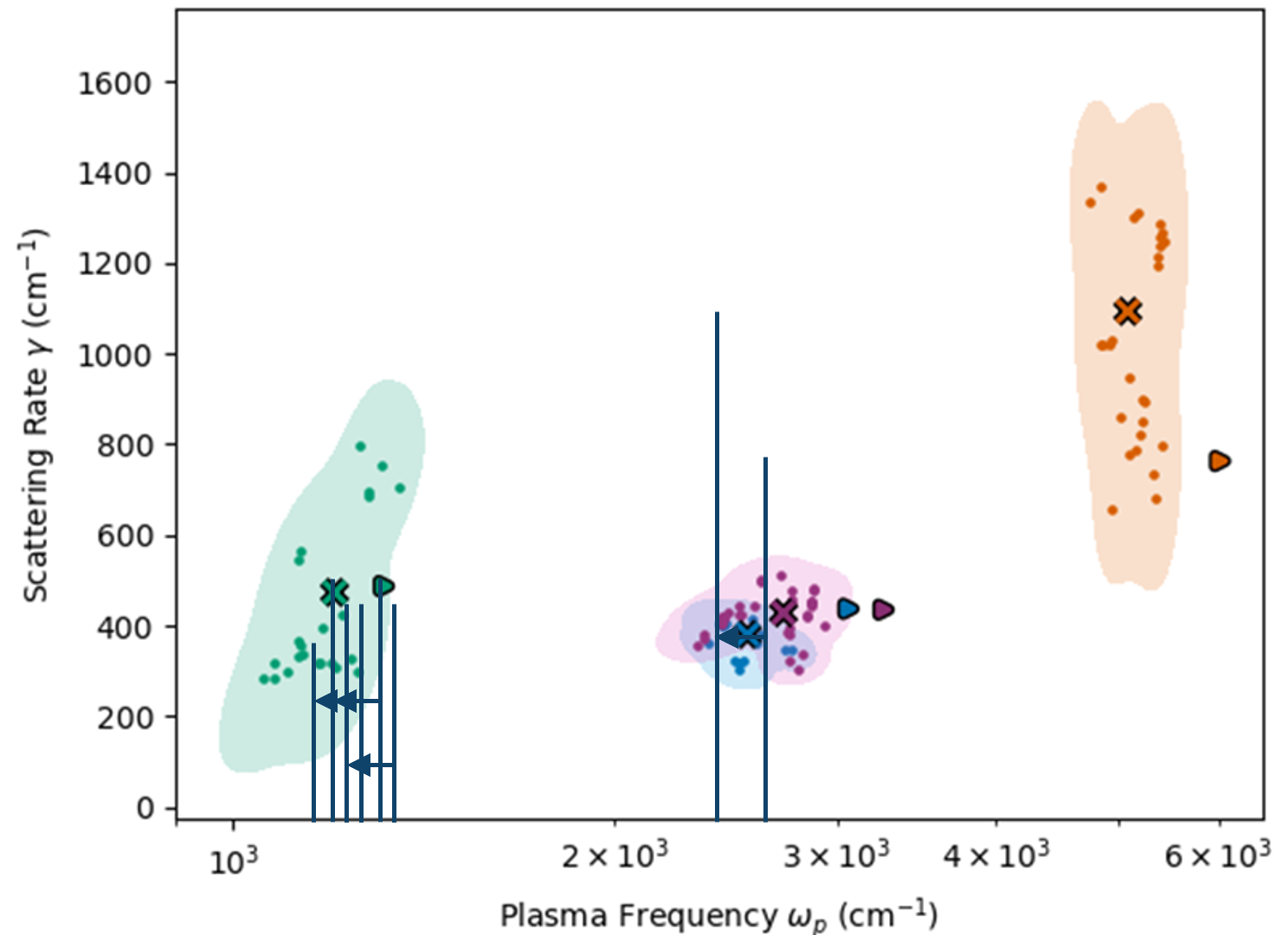
Comparison between infrared (IR) nanospectroscopy (dots + crosses) and conventional IR spectroscopy (triangles) confirms accuracy and precision for determining nanoscale electronic properties. It also reveals a consistent decrease in plasma frequency, consistent with a surface depletion layer.
The Science
Synchrotron infrared nanospectroscopy shows promise for measuring the electronic properties of nanoscale semiconductors that are challenging to measure using existing methods.
The Impact
The approach could eventually be applied as a precision tool to measure other advanced materials used in next-generation electronics.
Summary
Semiconductors are useful materials that have properties which allow researchers to control the flow of electrical charge. This is typically done by changing how many charge carriers are available and how freely they can move. Semiconductors are essential components for computer chips, smartphones, and many other electronic devices. As semiconductor technology shrinks down to the nanoscale, measuring the electronic properties of these materials has become more challenging. Existing methods are able to measure carrier concentration, but have a harder time measuring the scattering rate, how frequently those carriers are scattered as they move through the material. Infrared spectroscopy can measure both of these properties, but the resolution is limited when looking at semiconductors at the nanoscale.
To address this limitation, a research team led by scientists at the National Synchrotron Light Source II (NSLS-II), a U.S. Department of Energy (DOE) Office of Science user facility at DOE’s Brookhaven National Laboratory, used synchrotron infrared nanospectroscopy at NSLS-II’s Magnetic, Ellipsometric, Time-resolved Infrared and Nanospectroscopies (MET) beamline to combine extremely bright, broad-spectrum infrared light with an atomic force microscope to probe areas roughly 10 nanometers across, small enough to study the features of modern semiconductor devices. By analyzing how the infrared signal changes across a broad range of frequencies, researchers can determine local electronic properties of a semiconductor, including the concentration of mobile charge carriers and how easily those carriers move through the material
Tests on silicon samples showed that the nanoscale measurements generally agreed well with conventional infrared measurements, demonstrating that the approach can provide reliable quantitative information rather than simply showing differences from place to place. They also noticed that the nanoscale measurements detected about 30% fewer charge carriers near the silicon surface than measurements that probed deeper into the material. This may suggest a phenomenon called surface depletion, where fewer mobile charges are present close to the surface.
This work establishes synchrotron infrared nanospectroscopy as a promising tool for quantitatively examining semiconductor electronics at the nanoscale. Beyond silicon, the approach could eventually be applied to other advanced materials used in next-generation electronics.
Download the research summary slide (PDF)
Related Links
Paper: Quantitative Infrared-to-Terahertz Nanospectroscopy of Semiconductors
Contact
Lukas Wehmeier
Brookhaven National Laboratory
lwehmeier@bnl.gov
Mengkun Liu
Brookhaven National Laboratory, Stony Brook University
mengkun.liu@stonybrook.edu
G.L. Carr
Brookhaven National Laboratory
carr@bnl.gov
Publications
L. Wehmeier, Z. Zhou, M. Tsuneto, H. Zhao, S. N. Gilbert Corder, H.A. Bechtel, V. A. Martinez, C. C. Homes, D. N. Basov, M. Liu, and G. L. Carr, “Quantitative Infrared-to-Terahertz Nanospectroscopy of Semiconductors”, ACS photonics, 13 (16), 4902-4913 (2026). https://doi.org/10.1021/acsphotonics.6c01553
Funding
M.L. and D.N.B. acknowledge the Programmable Quantum Materials (Pro-QM) Energy Frontier Research Center (EFRC), funded by the U.S. Department of Energy (DOE), Office of Science, Basic Energy Sciences (BES), under award no. DE-SC0019443, for support of the data analysis. Near-field instrument construction at BNL was supported by the U.S. Department of Energy, Office of Science, National Quantum Information Science Research Centers, Co-design Center for Quantum Advantage (C2QA) under award no. DE-SC0012704. L.W. acknowledges funding by Empire State Development Corporation of New York. Synchrotron-based infrared nanospectroscopy was performed at the MET beamline of the National Synchrotron Light Source II, a U.S. Department of Energy (DOE) Office of Science User Facility operated for the DOE Office of Science by Brookhaven National Laboratory under award no. DE-SC0012704. Synchrotron-based infrared nanospectroscopy was also performed at Beamline 2.4 of the Advanced Light Source, a U.S. DOE Office of Science User Facility under contract no. DE-AC02–05CH11231.
2026-23231 | INT/EXT | Newsroom