Molecular Beam Epitaxy of Superconducting Oxides Group
Facilities
At the core of this FWP are two unique Atomic-Layer-by-Layer Molecular Beam Epitaxy (ALL-MBE) synthesis systems, illustrated in Figs. 1-3 below.
1. MBE-1: the 16-source ALL-MBE system in Bldg. 480
The first of these two is the ALL-MBE system originally designed and constructed by I. Bozovic with his team at Oxxel GmbH, Bremen, Germany, and subsequently acquired by BNL. This multi-chamber system consists of a 16-source MBE synthesis module interconnected by a 20-feet long UHV transfer chamber to the processing module in the neighboring clean-room lithography laboratory.
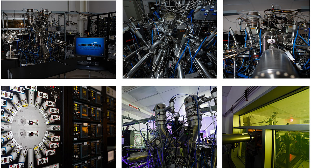
Figure 1. The 16-source ALL-MBE system in Bldg. 480. The synthesis chamber shown here is connected under UHV to the processing chamber in the clean-room lithography laboratory.
The ALL-MBE growth module (Fig. 1) consists of the following. (i) An ultra-high vacuum chamber with 2 main (1,000 l/s) turbo-molecular pumps and 24 differential (70 l/s) pumps. (ii) A transfer mechanism to introduce samples from air into the growth chamber without venting the MBE, which includes an introduction chamber, a transfer chamber, vacuum controls, etc. (iii) A sample manipulator with 6 degrees of freedom (3 axes of translation, one rotation and two tilt adjustments), motorized and computer-controlled, carrying a sample heater with 4 individually controlled quartz lamps capable of heating the substrate to Ts = 750°C. (iv) A video camera for visual inspection of the heated sample and a two-color pyrometer used to monitor the substrate temperature, on a motorized platform. (v) A system for generation, collection and delivery of pure ozone. (vi) Sixteen evaporation sources, each equipped with an individual pumping station, a gate valve and a fast-acting shutter. (vii) A custom-made 16-channel atomic absorption spectroscopy (AAS) system for simultaneous monitoring of source rates in real time. (viii) A quartz-crystal oscillator monitor (QCM), mounted on a separate manipulator with 3 translation degrees of freedom, motorized and computer controlled, which can be placed at the sample position to measure the deposition rate, or scanned across the area where films are deposited to measure the rate gradients. (ix) A reflection high-energy electron diffraction (RHEED) with sample scanning capability. (x) A time-of-flight ion scattering and recoil spectroscopy (TOF-ISARS) system for real-time chemical analysis of the film surface. (xi) A custom-made automatic operation control system that runs the vacuum valves, the roughening and turbo-molecular pumps, all motorized motions, the pneumatic shutters, the power supplies for thermal evaporation sources, the substrate heater lamps, and the ozone source.
2. MBE-2: the 8-source oxide MBE module of the OASIS system in Bldg. 734
The second is the oxide molecular beam epitaxy (OMBE) module integrated with the ARPES and the SI-STIM modules within the OASIS system, see Fig.2. It was designed based on the same (modular) general principle of operation as the standalone MBE-1 system described above, but here the design has been modified and adapted specifically for the needs of the OASIS system, including seamless integration with the other two modules, each of which imposed additional constraints and requirements.
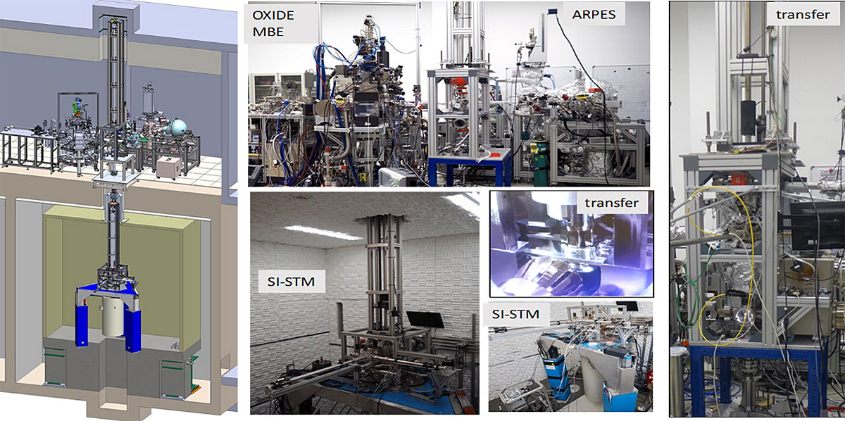
Figure 2. The OASIS system in Bldg. 745 consists of the 8-source oxide MBE module interconnected under UHV to the central transfer chamber and the ARPES module on the same (ground) floor, and to the SI-STM module located in an ultra-low-vibration underground vault below.
The OASIS OMBE system consists of the following components. (i) A UHV main chamber equipped with a 1600 l/s turbo-molecular pump and an ion pump; (ii) A set of 8 separate UHV chambers (‘arms’), each featuring a gate valve to the main chamber, a water-cooled spool, a pneumatic shutter, a differential turbo-molecular pump (80 l/s), and a thermal effusion cell; (iii) A two-stage load-lock allowing to insert samples from air and store up to 6 samples in its first (HV) and second (UHV) chambers; (iv) A unique sample transfer system interconnecting the load-lock, main chamber, and the rest of OASIS system by means of magnetically coupled manipulators, specifically designed for OASIS sample holder handling; (v) A sample manipulator with 6 degrees of freedom (three axes of translation, one rotation and two tilt adjustments), water cooled, motorized, and computer-controlled; (vi) A UHV-compatible infrared heater with up to 2 kW of infrared power delivered to the substrate via a set of gold spheroid mirrors, a pair of quartz rods and a water-cooled UHV viewport; (vii) An ultrapure ozone generation, collection, and delivery system with a cryogenic condenser and a valved ozone injector; (viii) A system of 8 quartz crystal monitors (QCMs) – one per each effusion cell – allowing to monitor the flux of each cell individually; (ix) An in-situ reflection high-energy electron diffraction (RHEED) system; (x) A custom-made network-based distributed automation system allowing for real-time recipe-based control of shutters, interlocked operation of gate valves and mechanical components of sample transfer system, automated drift-compensated flux calibration with QCM, real-time measurements with RHEED, monitoring of vacuum environment, and logging of all support infrastructure peripherals.
3. Lithography laboratory
The 16-source ALL-MBE is connected under UHV to another vacuum chamber devoted to in-situ lithographic processing, including ion-beam etching and electron-beam deposition of metallization and insulation layers, see Fig. 3. It is equipped with an IonTech 2-inch ion source and a 5-source Thermionics electron-beam evaporator. This chamber is installed in the clean room, so that substrates can be prepared in a class-100 clean environment and loaded into the system without surface contamination.
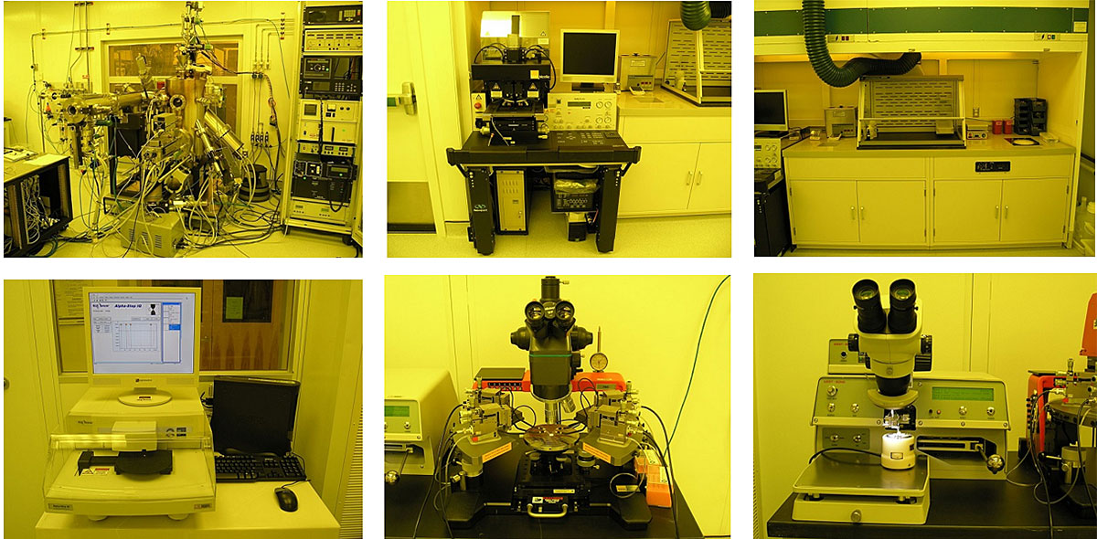
Figure 3. Lithography Laboratory, including the processing chamber of the BNL MBE system
The growth chamber and the processing chambers are connected via a transfer chamber, which has load-locks on both ends, supplied with quartz lamps for fast outgassing of substrates when they are first introduced into the vacuum system. Loading can be accomplished within minutes. The transport chamber is also equipped with ion pumps and Ti-sublimation pumps and has been tested to maintain vacuum down to 10-11 Torr (after bake-out, for which there is a panel box). It can be used for storage of 18 substrate holders, 3” in diameter.
4. Structural characterization tools: XRD and AFM
For determination of the crystallographic structure of films, the MBE group has a PANalytical Xpert Pro X-ray diffractometer (XRD), see Fig. 4a. This is a high-resolution (down to 5 arcsec) 4-circle goniometer which allows the study of in-plane and out-of-plane lattice constants, pole figures, rocking curves, grazing-angle reflectance, etc.
We also own and operate two Atomic Force Microscope (AFM) systems. In Fig. 4b we show a Nanoscope-III system located in Bldg. 480. In Fig. 4c we show a Nanoscope-IIIa system located in Bldg. 734. Both AFM systems are used on a daily basis to study the surface morphology and measure the surface roughness of substrates and films.
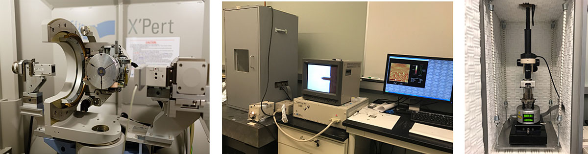
Figure 4. (a) PANalytical Xpert Pro 4-circle X-Ray diffractometer. (b) Digital Instruments Nanoscope IIIa AFM. (c) Nanoscope III AFM.
5. Transport property measurement systems
We have designed and built our own thin-film testing and cryogenic device-testing capabilities, including four liquid He4-based setups for R(T) and c(T) measurements (Fig. 5a,b) in the temperature range from 300 K down to 4 K. Three of these setups are motorized for automatic operation and remote control, greatly enhancing utilization and productivity. We also have two closed-cycle cryocooler systems (Figs. 5c,d) which together with their compressors provide convenient sample mounting stages for low temperature experiments without daily consumption of liquid Helium. We have improved the design of the sample stages compared to the originals, and improved temperature stabilization by over two orders of magnitude ‑ their stability is now better than ±1 mK in the range of 3 K to 300 K.190
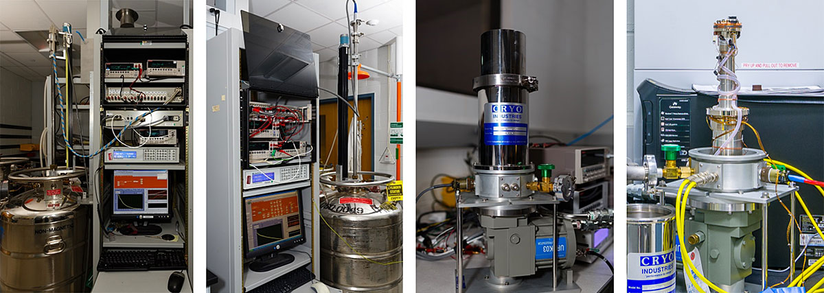
Figure 5. (a) A setup for measurements of resistivity as a function of temperature, down to 4 K. (b) A setup for measurements of mutual inductance vs. temperature, down to 4 K. (c) A closed-cycle cryocooler for transport or inductance measurements down to 3 K. (d) The sample stage of CCC with a custom-designed and built thermal stabilizer and a sample holder for transport measurements.
We have purchased and customized two top-loading He3 cryostats together with 9 T superconducting magnets from Cryo Industry of America, Inc., see Figs. 6a,b. They enable us to tune the sample temperature from 300 K down to 300 mK with a temperature stability of ±0.1 mK, and apply a magnetic field from 0 T to 9 T. With our customized design of the sample probes, we can conduct a variety of experiments measuring different physics quantities, e.g. mutual inductance, resistivity, or the Hall effect. A helium liquefier (Fig. 6e) captures and liquefies the boil-off from these two systems, which has significantly reduced the amount of liquid helium consumed when operating this equipment.
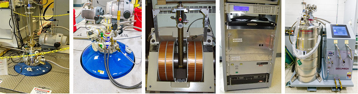
Figure 6. (a, b) 0.3 K, 9 T He3 systems. (c, d) 32-channel He4 system with 1.1 T magnet. (e) The liquid helium recovery plant.
Next, we have built another set-up for multi-channel (parallel) measurements of R(T) and of the Hall effect. It uses a conventional 1.1 T electromagnet, Fig. 6c. Our home-built 32-channel analog and digital lock-in electronics (Fig. 6d) can output a low-frequency ac current and measure ac voltages at 32 channels in parallel, with sub-microvolt accuracy. It lowers the cost and time consumption to acquire high quality transport data and increases the efficiency of our measurements by a factor of ~30. It is equipped with a home-built multiplexer for easy switching between longitudinal resistivity and Hall resistivity measurements.
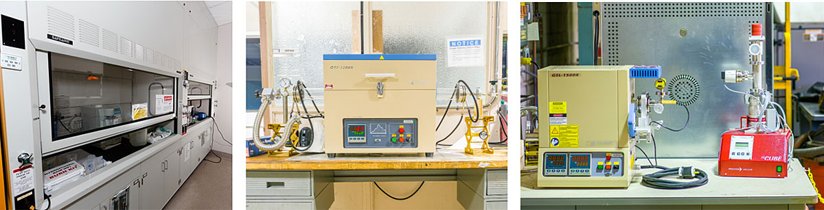
Figure 7. (a) Chemistry Laboratory. (b) Tube furnace. (c) Rapid thermal annealing furnace
6. Other processing and characterization facilities
In Fig. 7a, we show our Chemistry Laboratory, where we clean and etch substrates and MBE parts to be inserted into ultra-high vacuum. Fig. 7b shows a split-tube furnace capable of reaching 1200 0C that we use to perform ex-situ annealing experiments after film growth. Fig. 7c shows another furnace, designed to allow for rapid thermal processing with a maximum working temperature of 1500 0C.
Fig. 8a shows a high-pressure oxygen tube furnace that can reach the pressure of 200 atm and the temperature of 1,100 0C. The sample tube, made of a special Ni-based super-alloy, has an inner space of 20 mm diameter and 550 mm length, so it can accommodate more than 50 samples at the same time. The temperature and the pressure of the furnace are monitored and controlled from a remote computer for maximum safety. Fig. 8b shows a custom-built ozone-annealing chamber for post-growth annealing of samples with temperature as high as 800oC and ozone pressure in the mTorr range. The long-time annealing (from hours to weeks) is beneficial for the improvement of film crystalline coherence and electronic uniformity. Fig. 8c shows a multi-target sputtering system, which we have upgraded and commissioned, and have been using for deposition of ruthenates, tungstates and cobaltates. Fig. 8d shows a thermal evaporation system used for deposition of metallic contacts (mostly Au or Ag) onto MBE-grown or sputtered films, for transport measurements.
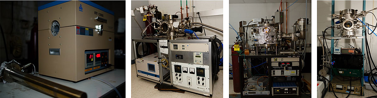
Figure 8. (a) The high-pressure furnace. (b) The ozone-annealing chamber. (c) The sputtering system. (d) The thermal evaporator.
7. User facilities
We employ a range of other tools for nanofabrication (such as electron-beam lithography, reactive ion etching, sputtering of contact layers, and focused ion beam lithography) and for characterization of thin films and devices (scanning electron microscopes, LEEM and PEEM) at CFN user facilities in BNL. We also collaborate with various other groups at BNL, leveraging on their unique experimental facilities such as high-resolution (< 0.8 Å) transmission electron microscopes (the total of 6 instruments at CMPMS and CFN), unique x-ray scattering setups at NSLS-2, ultrafast electron diffraction, etc. Additionally, we are regular users of high-field (31 T dc, 60 T and 90 T pulsed) magnets at National High Magnetic Field Laboratories in Tallahassee, FL and Los Alamos National Laboratory, and the French National High Magnetic Field Laboratory in Grenoble, France.
Brookhaven Science Associates
Brookhaven Science Associates manages and operates Brookhaven National Laboratory on behalf of the U.S. Department of Energy's Office of Science. BSA is a partnership between Battelle and The Research Foundation for the State University of New York on behalf of Stony Brook University. | More