CFN User Spotlight: Jennifer Carpena-Núñez Studies the Fundamentals of Carbon Nanotube Growth
interview with a CFN user
August 28, 2018
 enlarge
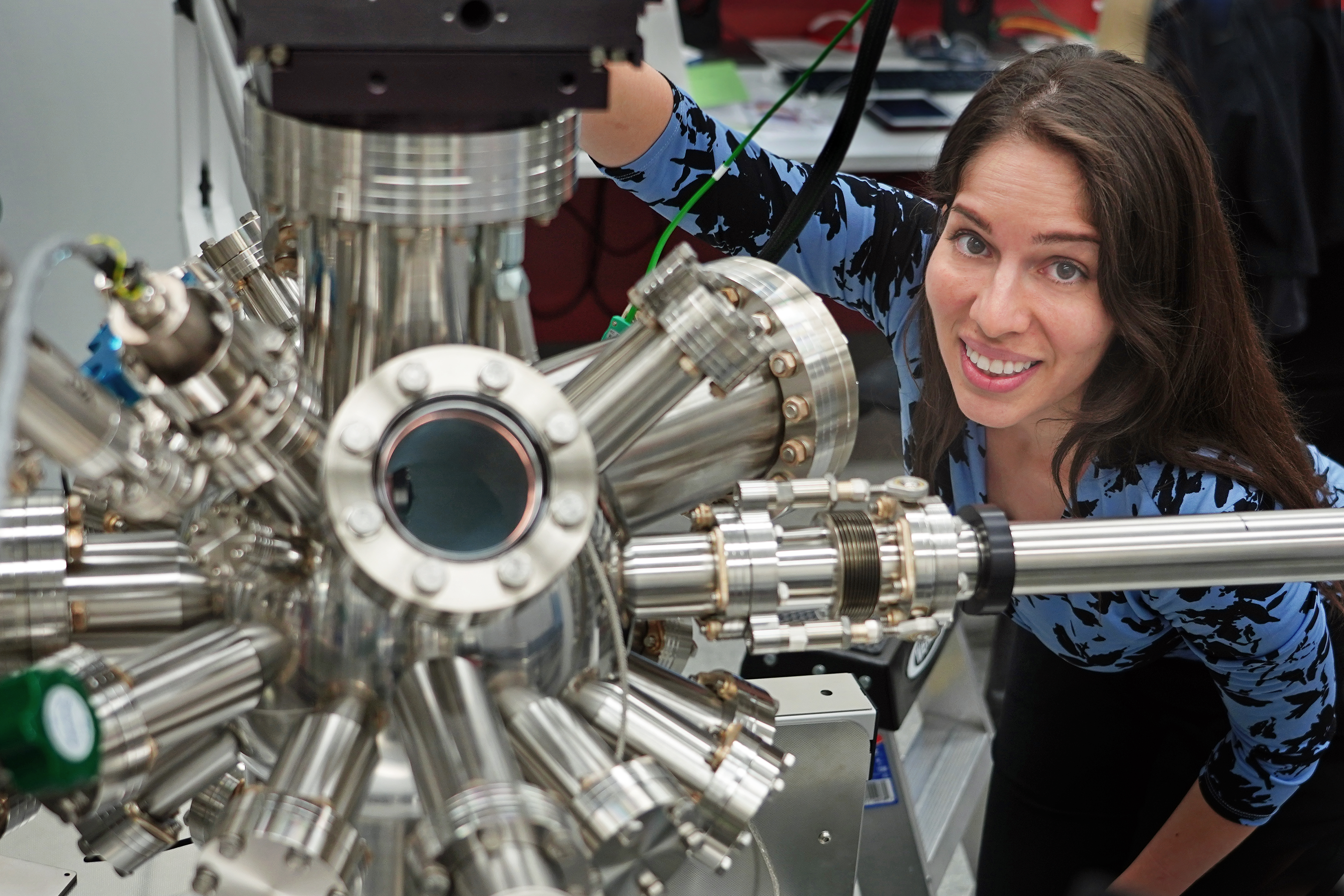
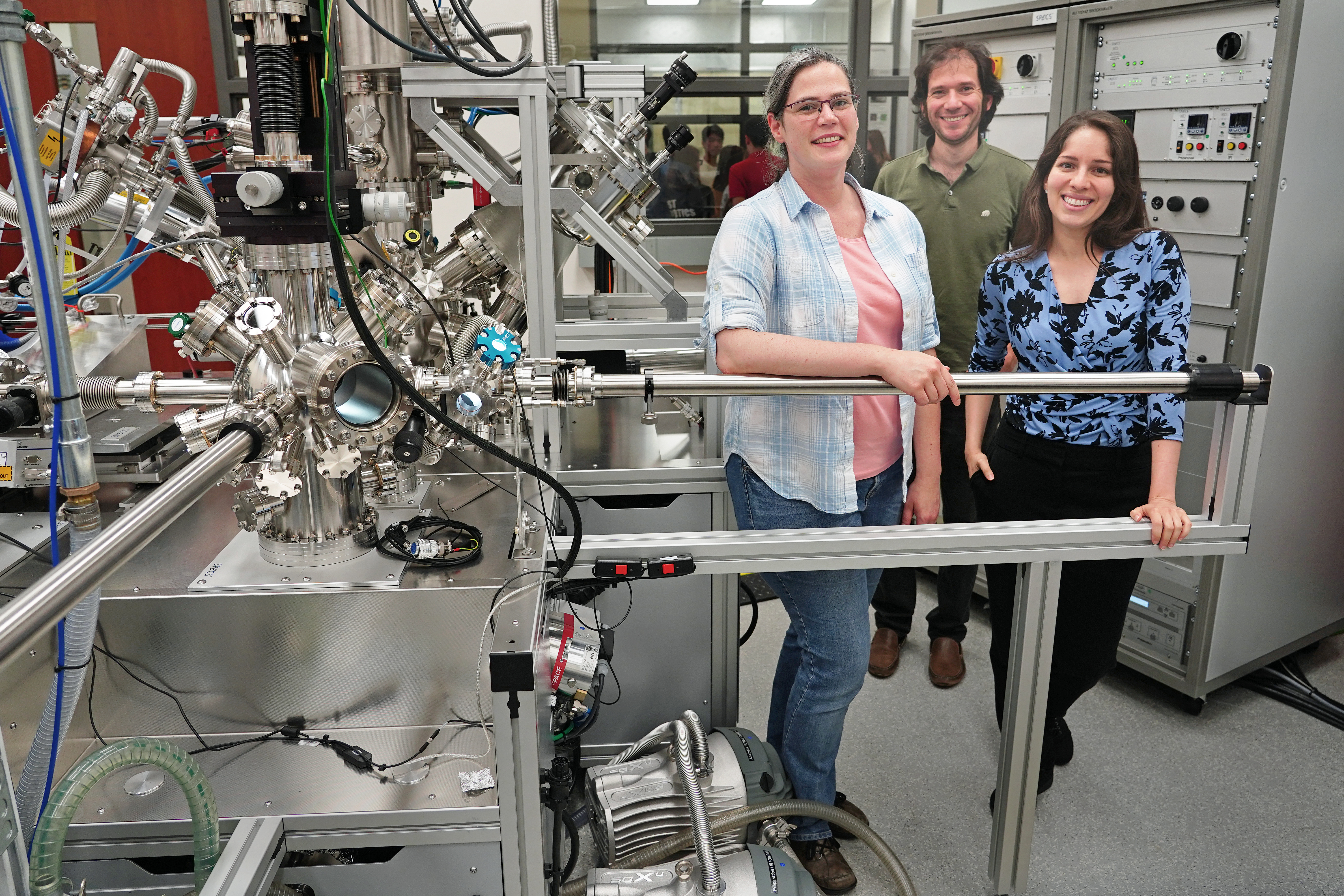
Jennifer Carpena-Núñez next to the new ambient-pressure x-ray photoelectron spectroscopy system at Brookhaven Lab's Center for Functional Nanomaterials. She uses this instrument to study the chemical composition of catalyst systems used for carbon nanotube growth, which are cylindrical structures that are only a few billionths of a meter in diameter.
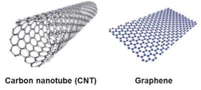
Carbon is a special element because of the different ways its atoms can bond together. These “allotropes” of carbon are chemically identical but physically very different. In recent years, chemists have been trying to synthesize new forms of carbon with useful mechanical, electrical, thermal, optical, and magnetic properties. Chemical physicist Jennifer Carpena-Núñez—a postdoctoral research associate in the Interface Science and Catalysis Group at the Center for Functional Nanomaterials (CFN), a U.S. Department of Energy (DOE) Office of Science User Facility at Brookhaven National Laboratory, and at the Materials and Manufacturing Directorate at the U.S. Air Force Research Laboratory (AFRL), a Department of Defense research laboratory at Wright-Patterson Air Force Base in Ohio—has been synthesizing and characterizing carbon nanotubes. Made from thin sheets of graphitic carbon rolled into long hollow tubes, these cylindrical structures are incredibly strong, lightweight, and flexible, and they are excellent conductors of heat and electricity. Owing to their “supermaterial” properties, carbon nanotubes are attractive for many applications, such as energy storage, biological and chemical sensors, electronic devices, and aircraft components.
The U.S. Air Force Research Laboratory leads the discovery, development, and delivery of new air, space, and cyberspace technologies to defend our country. Why is AFRL interested in carbon nanotubes?
One of the research goals at AFRL is to improve the performance of their aircraft. Using carbon nanotubes in aircraft components such as electrical wiring and structural composites could help reduce the amount of weight on the aircraft, thus leading to better fuel efficiency.
Another research goal is to improve the performance and safety of warfighters. Minimizing the amount of weight they have to carry in batteries to power their displays, satellite radios, computers, and other electronic devices is key to achieving this goal. Traditionally, battery cathodes and anodes are made with activated carbon, and as a result, they tend to be heavy. Basically, there is a hunk of carbon with pores where the active materials for the electrochemical charge and discharge reactions can permeate. The Air Force wants to replace these components with more lightweight materials. Because they are somewhat porous and conduct very well, paper-thin sheets of carbon nanotubes are excellent candidates to replace the anodes and cathodes of batteries so that the overall weight of the battery can be reduced. Carbon nanotubes are also extremely flexible. This property is important to the growing field of wearable technologies, which not only need to be very thin but also able to sustain repeated folding and bending. In addition, carbon nanotubes can be in molecular sensors for the detection of biological or chemical species. Carbon nanotubes improve the sensitivity of certain molecules, allowing for earlier detection of, for example, neurotoxic gases in aircraft cabins or biometrics of a pilot. These are extremely important applications of carbon nanotubes, as one of AFRLs most crucial missions is to support our airmen and airwomen and ensure their safety.
How do you make carbon nanotubes?
Synthesizing carbon nanotubes is a little bit like following a cooking recipe—there are key ingredients and an overall general guideline.
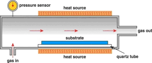
Usually, carbon nanotubes have three main ingredients: a source of heat, a source of carbon (typically a hydrocarbon), and a catalyst. You can grow the nanotubes using various synthesis techniques, but the method I use is called chemical vapor deposition. Essentially, you place your catalyst in a furnace, heat the catalyst to a certain temperature, and flow in the hydrocarbon through a gas inlet. But first, you must transform your catalyst to a specific chemical state. This transformation is achieved by some type of pretreatment, such as by exposing it to a reducing environment so that it is in its fully metallic state (no oxygen is bound to the metal). There are other things you can do to enhance the catalyst growth process. Before I arrived at AFRL, there were significant efforts in improving how catalysts grow by adding things like water, which extends the lifetime of the catalyst. One of my ongoing research projects is to study at a fundamental level what makes a catalyst grow and why one catalyst grows better than another.
After activating the catalyst, you “incubate” the catalyst. Some of the carbon becomes soluble in the catalyst and will saturate to get ready to form a nanotube in a process called cap formation. Following this nucleation, the carbon cap detaches from the catalyst and becomes a tube. Then, the tube starts growing, with the extent of growth generally determined by the catalyst lifetime. The final step is termination, when the tube stops growing. Many of these growth stages continue to be active areas of current research. For instance, if scientists can determine what causes termination, then they can try to prevent it or perhaps extend the catalyst lifetime.
What kinds of catalysts do you use?
The catalyst can either be unsupported, sort of like a powder, or bound to a support system made of materials such as silicon dioxide or aluminum oxide. For bound catalyst systems, the support materials modify the properties of the catalyst and thus impact the growth of carbon nanotubes. For example, one of my coworkers at AFRL demonstrated how ions can induce changes in the surface properties of a support material that will allow the catalyst/support system to become active for carbon nanotube synthesis.
 enlarge
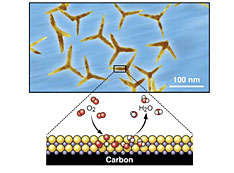
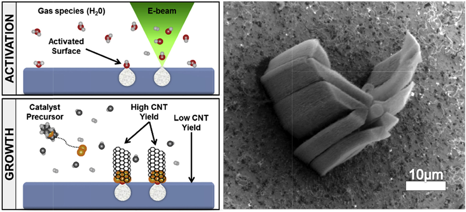
(Left) An illustration showing carbon nanotube (CNT) growth using e-beam induced chemistry. The yield is only high in regions where the surface was activated. (Right) A scanning electron microscope image of a pattern of the U.S. Air Force logo. From Carbon 135 (2018), 270–277.
My AFRL colleagues and I conducted the “sequel” to this project. Instead of bombarding the support surface with ions to activate the surface, we used electrons through a process we developed, called e-beam induced chemistry, and for which we have submitted a patent. This process is very similar to traditional lithography, in which an electron beam is used to write—or not write—a pattern onto a substrate. Microelectronic components like computer chips are the product of lithography. But with e-beam induced chemistry, instead of the electrons hitting a resist to transfer the pattern to a substrate, they interact with the support surface.
In our case, we were using an inactive sapphire surface, which is not a good catalyst support. We placed the sapphire surface in an environmental scanning electron microscope (SEM), or variable-pressure SEM, at AFRL, and this system allowed us to image the sample with an electron beam in an environment of water vapor. Traditional SEMs work under high vacuum, but with the environmental SEM we were able to have gas filling in the chamber. Environmental (or variable-pressure) SEMs are typically used to help reduce charging—a phenomenon that occurs when charges from high-energy electrons build up on the surface of an insulating material. Charging is problematic because it can distort the resulting image.
In this study, we used an electron beam in the presence of water vapor to activate the sapphire support for an iron catalyst. Because we can control the electron beam, we were able to not only activate the support surface but also to select which regions of the surface were activated. Carbon nanotube growth then takes place selectively in the activated regions.
Why is it important to have the ability to control which areas of the catalyst support surface get activated?
One of the main applications of carbon nanotubes is electronics. For that type of application, 100 percent coverage of a conducting material on the surface may not be desirable. For example, maybe you want specific patterns that have carbon nanotubes acting as conductive paths on certain areas of the surface while other areas are insulating.
The part that really excites me is the general idea of using an electron beam to control the chemistry of the support surface, chemically modifying it in such a way that activates the catalyst support exclusively at the patterned regions. A significant component of the project involving activation of sapphire for carbon nanotube growth was to understand what we were doing with our technique and how we were doing it. Once we have this understanding, we can then think more about applications of the technique. Our group at AFRL is now exploring e-beam induced chemistry for creating other surface chemistries.
The Electron Microscopy Facility at the CFN has a variety of high-resolution transmission electron microscopes (TEMs)—do you use any of those instruments for your research?
Yes, the CFN has an environmental TEM in which you can flow gases into the chamber, similar to what we did with the SEM. Transmission electron microscopes are, in general, an essential component of materials research. With an environmental TEM, we can induce e-beam chemistries, analogous to those induced in the environmental SEM, with two main advantages: we can do so with increased spatial resolution, so our pattern features can be made smaller, and we can induce our chemistry and both visualize and analyze the nature of the process in real time via techniques such as electron energy-loss spectroscopy. So, observing the same process of carbon nanotube growth in the environmental TEM was a no brainer. Plus, there was already a multiyear collaboration in place between AFRL and the CFN. Benji Maruyama, who leads research on carbon nanotubes at AFRL; Eric Stach, who at the time led the Electron Microscopy Group at the CFN; and Dmitri Zakharov, staff scientist in the Electron Microscopy Group at the CFN, had collaborated on several environmental TEM studies looking at the fundamentals of carbon nanotube growth. My AFRL coworkers and I are continuing this collaborative effort between AFRL and the CFN.
Benji is actually how I joined AFRL in 2014. I had met him that year while presenting a poster at a Materials Research Society conference. At the time, I was doing carbon nanotube research through a NASA [National Aeronautics and Space Administration] Space Technology Research Fellowship. My mentor at NASA was Emilie (Mia) Siochi, a senior materials scientist at NASA Langley Research Center, and Benji was familiar with her work. When he came to look at our poster, he asked if I was interested in doing a postdoc. I submitted a proposal to conduct carbon nanotube research to the National Research Council, which offers postdoctoral associateships at national labs and other federal institutions through the Research Associateship Program. I was recommended for the associateship and participated in the program for a duration of three years.
It sounds like you do a lot of electron microscopy studies, yet you are part of the Interface Science and Catalysis Group at the CFN. How does your carbon nanotubes research relate to this group?
CFN scientists came up with the idea that the expertise between the Electron Microscopy and the Interface Science and Catalysis Groups could be merged, as carbon nanotube growth is in essence a catalytic process. As a result of that initial idea of merging these two workflows, I joined the Interface Science and Catalysis Group, currently led by Dario Stacchiola. This group works on many catalyst models, one of which is called zeolites. Particularly, we are working on 2D zeolite frameworks made of silicates (composed of silicon and oxygen) and aluminosilicates (composed of aluminum, silicon, oxygen). As I mentioned earlier, one of the catalyst support systems I study is silicon oxide. Because some of these zeolites are composed of silicates, which are a form of silicon oxide, we are exploring the possibility of using zeolites to support catalysts for carbon nanotube growth.
Another reason the groups came together is because of a collaboration between Eric Stach (now at UPenn), Dario, and Klaus Attenkofer, who is responsible for the hard x-ray spectroscopy program at Brookhaven’s National Synchrotron Light Source II (NSLS-II) [another DOE Office of Science User Facility]. They had an idea to design a universal experimental cell that could be used across different platforms, without having incompatibilities in the sample types or geometries, or in the environmental conditions. Typically, samples have to be prepared and tuned for each instrument. Similarly, when you go from one instrument to the next, the gas species, pressures, and temperature ranges may not be the same. For example, some instruments require high vacuum. When you have different techniques with different requirements, you can end up with very different results. So, you are not always comparing apples to apples. This experimental cell, which is currently being designed by NSLS-II engineer Yi Zhu, will help us close the experimental gap between the techniques.
Do you use any other facilities on site at Brookhaven?
Yes, I do ambient-pressure x-ray photoelectron spectroscopy (AP-XPS) experiments at one of the NSLS-II beamlines to understand the chemical composition of my samples. The environmental TEM provides sufficient time resolution to look at the microstructure of the carbon nanotubes during their different stages of growth, but this imaging tool is not ideal when it comes to observing what is happening chemically.
As I mentioned before, there are six basic stages of growth: catalyst activation, catalyst incubation, cap formation, tube nucleation, tube growth, and tube termination. The timescale for the first and second steps depends on the chemistry of the catalyst and the environment to which the catalyst is exposed. Steps three and four are on the order of one to ten seconds. In most cases, a few seconds is not long enough to capture information about the chemistry of a system. But for NSLS-II, it is. Because it is a super-bright source of x-rays, I can get the signal in a matter of seconds after irradiating my samples. I am currently doing a series of studies looking at the chemical state of different catalysts, trying to pin down which oxidation state is responsible for their catalytic activity and carbon nanotube growth. Our goal is to identify which condition or set of conditions determines whether one catalyst particle grows or not.
We have recently started integrating the new lab-based AP-XPS system at the CFN into our studies. This system, managed by CFN staff scientist Ashley Head, has similar capabilities as the one at NSLS-II—it can flow gases, has excellent energy resolution, and decent time resolution. We plan to use this system to grow carbon nanotubes, using zeolites as the catalyst support system.
 enlarge
Jennifer Carpena-Núñez (right) and CFN colleagues Ashley Head and Anibal Boscoboinik, both of the Interface Science and Catalysis Group, with the new ambient-pressure x-ray photoelectron spectroscopy instrument at the CFN.
We are also trying to expand my carbon nanotube synthesis work to other forms of spectroscopy, such as x-ray absorption near-edge structure (XANES) spectroscopy. While AP-XPS gives you information like the oxidation state of the catalyst, XANES provides a bit more specific information about local environments. In particular, XANES can be used to determine local structure—which atoms are next to each other, what is the nearest-neighbor distance, and what kind of symmetry is present.
Combining the results of AP-XPS, XANES, and TEM gives you a complete picture of what is going on in a system. That is the really cool part about the CFN—all in one place, you have these state-of-the-art instruments that you cannot find elsewhere. More importantly, you can have access to them if you write a successful proposal.
A theme of your research seems to be next-generation materials for aerospace. Is aerospace an interest of yours?
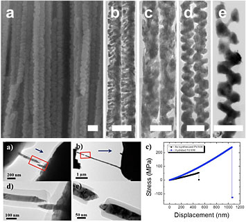
(Top panel) A scanning electron microscope image of palladium and copper nanowire arrays with screw-threaded shapes (a), and transmission electron microscope images of the nanowires with random-chapped (b), random-gapped (c), screw-threaded (d), and spiral (e) shapes. The scale bars are all 100 nanometers. (Bottom panel) Tensile failure of as-synthesized (a and d) and hydrogen-exposed (b and e) palladium nanowires, showing ductile and brittle failure, respectively. The corresponding stress measurements show stiffening of the hydrogen-exposed nanowires (blue curve in c). From Scientific Reports 4, no. 3773 (2014) and its supporting documentation.
As a kid, I dreamt of someday working for NASA. I think that the factor that likely contributed to this dream is that, when I was growing up in Puerto Rico, my mom would bring my brothers and I outside at night to lay down on a sheet in our backyard so we could look at the stars. She would talk about the different stars we were observing, and I developed a fascination with space science and telescopes.
For my bachelor’s degree, I entered the physics program at the University of Puerto Rico, Rio Piedras Campus, with the idea that I was going to pursue astronomy. In my third year as an undergraduate, I joined the research group of Professor Luis Fonseca, a nanoscientist. I continued doing research with the same professor while pursuing my master’s degree in physics and PhD in chemical physics. Along the way, I did seven internships with NASA. My exposure to nanomaterials research through these internships and in Professor Fonesca’s lab shifted my interest from astronomy to nanoscience. In the lab, I started getting into materials characterization via electron microscopy.
 enlarge
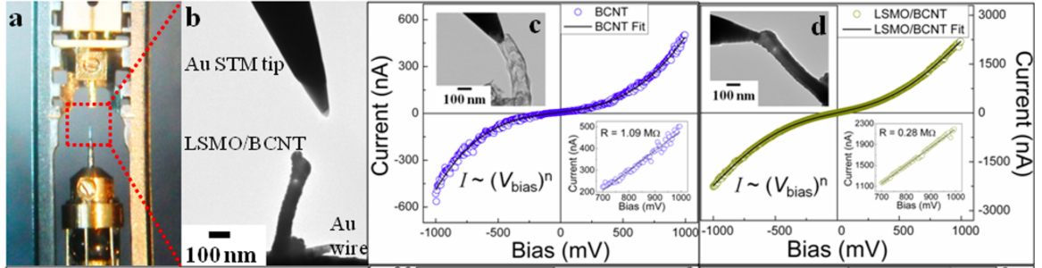
Electrical conductivity measurements of nanostructures using an in situ transmission electron microscope setup (a and b). The bare (c) and coated (d) bamboo carbon nanotubes (BCNT) show distinct electrical behavior. The coating material, lanthanum strontium magnetite (LSMO), makes the tubes more conducting. From Carbon 65, 252–260 (2013).
For my master’s and PhD theses, I did a lot of in situ TEM studies where I looked at the mechanical and electrical properties of a variety of nanostructures—in particular, palladium nanowires for hydrogen sensors (master’s degree) and carbon nanotubes as matrix components in composite materials (PhD). For example, through one of my projects funded through NASA, I was looking at the compressive and tensile properties of carbon nanotubes—in other words, how much the structures can endure when you compact them or pull on them. NASA is involved in several research projects looking at carbon nanotube–reinforced composites for aerospace components, which need to be able to endure many different types of stress. Theoretically, carbon nanotubes have great mechanical properties, but in practice they do not meet expectations. While I was at NASA, my team focused on understanding why there was such a big gap between theory and practice.
So, now, instead of looking at the stars with a telescope, I am looking at materials with electron microscopes—a different kind of lens!
What is limiting the widespread adoption of carbon nanotubes in the real world?
 enlarge
Scanning electron microscope images at low (a) and high (b) magnification of a failure site after tensile testing of a polymer-infiltrated carbon nanotube paper. From Applied Materials & Interfaces 5 (2013): 8597–8606.
Carbon nanotubes are predicted to be incredibly strong because of their carbon-carbon bonds; however, many composites are made with polymer materials, and carbon nanotubes often times do not interact chemically with these materials. Because this interaction is very weak, what ends up happening is a phenomenon called phase separation. As a result of this phase separation, the composite will have carbon nanotube–rich and polymer-rich regions. Even if you have a well-dispersed uniform composite, the polymer could still act as the “weak link,” with its properties dominating. We often make use of the word “cross-linking” to refer to a strong interaction between the reinforcement element and the matrix. Whether carbon nanotubes are used as reinforcing elements or as the matrix, the goal is to cross-link them to either neighboring carbon nanotubes or polymer chains via strong interactions.
As I mentioned, one of the biggest issues is that polymers can act as the weak link in composites. This problem can be tackled by inverting the ratio between the matrix and reinforcement. Instead of carbon nanotubes being dispersed within a polymer matrix, as would be done in traditional composite fabrication, the polymer is imprinted onto matrices composed of carbon nanotubes. Two examples of these imprinted-polymer matrices are carbon nanotube sheets and yarns. The idea is that, instead of having lots of matrix material with reinforcing elements, you have lots of strong material (carbon nanotubes) that is reinforced with the polymer. With this arrangement, and by further processing to induce cross-linking, the resulting material has the desirable properties of the carbon nanotubes. This cross-linking carbon nanotube project was a big component of my graduate work. It involved a strong collaborative effort between academia, NASA, and Nanocomp Technologies, Inc., who made the sheets and yarns.
 enlarge
Scanning electron microscope image of a 33-percent-stretched carbon nanotube sheet after processing. Stretching during polymer infiltration helps improve load transfer between carbon nanotubes. From Applied Materials & Interfaces 5 (2013): 8597–8606.
One of the primary limitations in technology transfer of these carbon nanotube-based technologies is the inability to synthesize carbon nanotubes with desirable properties. This inability is in principle due to a lack of understanding. As I mentioned earlier, scientists still lack an understanding as to why some catalysts grow tubes while others do not. Another area that requires further advances is chirality control during carbon nanotube synthesis. Imagine folding a sheet of graphene and having the carbon atoms perfectly matched up, and then you start twisting that lattice—that is the chirality of the tube. Chirality is important because it determines the tube’s electronic properties, such as whether it is semiconducting or conducting. But we are not yet at the stage where we can control chirality at a large scale, and thus we cannot control the electronic properties that emerge. Control over synthesis at a large scale is critical for technology transfer.
A major hindrance outside of the materials themselves or control over synthesis is the amount of time it takes to run the experiments. For the chemical vapor deposition system in the lab, I can run maybe two or three experiments at once. Doing TEM, AP-XPS, or any of the other techniques takes about four hours per experiment. To tackle this issue in general, AFRL has a big effort in autonomous research setups, and this effort led to the development of the Autonomous Research System (ARES).
 enlarge
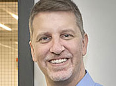
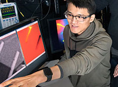
Benji Maruyama is the creator of AFRL's Autonomous Research System (ARES), which autonomously plans and runs experiments, performs in situ characterization, and analyzes experimental results.
ARES is particularly good at detecting when carbon nanotubes are growing, quantifying the yield and lifetime of the tubes, and determining the quality of the tubes (whether they are single, double, or multi-wall). Even more impressive, ARES can perform experiments on its own. ARES was trained via machine learning on previous growth experiments, and by determining which conditions led to a particular growth, the system can mimic those conditions to execute the experiment, ultimately reproducing the desired carbon nanotubes. So, if we want to grow a tube that has certain properties in terms of yield or quality, we can. Moreover, we can now run 100 or more experiments in a single day.
You mentioned that you grew up in Puerto Rico. How did growing up there impact your education and trajectory as a scientist?
Being where I am from led me to where I am today. I am considered a minority, and the support I have received as such was a big part of why I was able to conduct research over all these years. I have been very blessed to have received funding throughout my undergraduate and graduate studies, as it allowed me to focus entirely on my research. Not everyone is so fortunate. I remember many other students having to abandon their research work or even the graduate program altogether because they needed to support their families. Whenever I meet students, I almost immediately tell them about all of the funding sources and research opportunities that are available. Many of the students are not aware these opportunities even exist.
Are you involved with any student outreach programs?
I have recently become involved in outreach programs at Brookhaven Lab. This summer, I gave a seminar to a group of high-school science, technology, engineering, and mathematics (STEM) students who were participating in the Office of Educational Programs’ STEM-Prep Summer Institute (SPSI), a four-week program for underrepresented minority students. I gave a seminar during their physics week and introduced the students to nano and materials science, electron microscopy, and carbon nanotubes. The students were incredibly engaged and had many outstanding questions. I was very impressed by the SPSI program and its participants.
I also recently participated in Brookhaven’s Summer Sunday at the CFN. Summer Sundays allow community members to become familiar with the science being done at Brookhaven. It was exciting to see the response from the general audience, which included people of all ages. It was surprising to see just how many people are science advocates. It was even more exciting to see children and teenagers engaging in science at such an early age. I think such engagement is incredibly promising. Many of these kids were incredibly smart, and some of them already were expressing interest in becoming scientists in the future. I feel fortunate to be a part of this experience at Brookhaven. Summer Sundays and the SPSI program reminded me of why I became a scientist in the first place: to learn and discover.
2018-13091 | INT/EXT | Newsroom