At the Interface of Organic Chemistry and Nanotechnology with Adam Braunschweig
interview with a CFN user
May 21, 2020
 enlarge
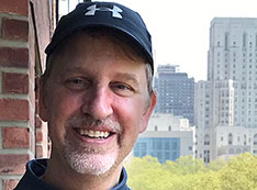
Adam Braunschweig leads a research group at the CUNY ASRC that solves energy, health, and environment problems at the interface of organic chemistry and nanotechnology.
Adam Braunschweig is an associate professor in the Nanoscience Initiative at the Advanced Science Research Center (ASCR) at The Graduate Center, City University of New York (CUNY), and an associate professor of chemistry and biochemistry at CUNY’s Hunter College. At the CUNY ASRC, he leads a team of postdocs and graduate and undergraduate students working to solve problems at the interface of organic chemistry and nanotechnology. About two years ago, their research on organic semiconductors for solar cells brought them to the U.S. Department of Energy’s (DOE) Brookhaven National Laboratory. Here, through the Center for Functional Nanomaterials (CFN) user program, they are leveraging the x-ray scattering capabilities of the CFN Advanced UV and X-ray Probes Facility. In particular, they are performing experiments at the Soft Matter Interfaces beamline—operated in partnership between CFN and the National Synchrotron Light Source II (NSLS-II)—to understand how the molecules in thin films of these organics pack together. This packing geometry directly impacts the electronic properties of the thin films when they are integrated as active layers into devices and irradiated with light or injected with electrical charges. Braunschweig holds a PhD in organic chemistry from the University of California, Los Angeles (UCLA), and a BA in chemistry from Cornell University. He joined the CUNY ASRC in 2016, following faculty appointments at the University of Miami (UMiami) and New York University (NYU).
What does research in the Braunschweig Group focus on?
My group is very problem oriented rather than method oriented. In other words, we apply any technique at our disposal to solve particular problems of interest. In general, we work on three areas at the interface of organic chemistry and nanotechnology.
The first is interactions between light and self-assembled nanostructured matter. We look at how self-assembly can drive emergent optoelectronic properties. We follow designs common in nature to reproduce natural emergent phenomena for applications like solar energy harvesting.
 enlarge
Andrew Levine is a PhD student in Braunschweig's group. He earned a BS in chemistry from Rensselaer Polytechnic Institute and an MS in science education from Boston College. Before beginning his PhD, he taught high school chemistry for five years. He became interested in solar energy through his mother, who worked in the industry.
Andrew Levine, a fourth-year chemistry PhD student in my group, has been synthesizing supramolecular assemblies driven mostly by hydrogen bonding interactions to direct specific packing arrangements of organic semiconductor molecules. The properties of organic semiconductors are easily tunable by substituting different functional groups in the molecules. And organic semiconductors do not require high-energy processes to crystallize like silicon, the material conventionally used to make solar cells. Andrew has been doing part of this research at NSLS-II through the CFN user program.
Along the same vein of following nature’s design, we just started the comparative animal mucus project. Every animal produces at least five different mucuses. Mucus is a material whose properties arise from organization at the molecular, nanometer, and millimeter length scales. Subtle differences in the structure of proteins that make up a mucus can render one mucus an adhesive, another a lubricant, and another a semipermeable barrier. For example, pygmy hippos live most of their lives in water. But when they’re out of the water, they shed a lot of mucus that keeps their skin hydrated and also has sunscreen-like properties. If we can understand how nature does it, then we can introduce principles from nature to design synthetic materials with similar properties.
Another focus of my group is making combinatorial biomolecular arrays by developing new printing tools. In this project, we build new instruments that can perform iterative chemical reactions on surfaces, where the feature diameters are in the nanoscale regime. The resulting arrays can be used for applications ranging from assessing single-cell genomics to driving stem cell differentiation.
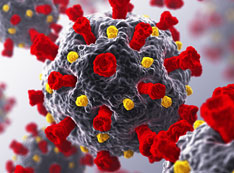
A final project involves the development of small molecules that selectively bind the carbohydrates found on the surfaces of cells and viruses. Right now, we’re integrating such molecules into sensors and therapeutics to mitigate the threat of the COVID-19 virus.
How do you go about taking this problem-oriented approach, which requires expertise in several different areas?
After I got my PhD in organic chemistry at UCLA, I spent nine months in Jerusalem for a visiting faculty position focusing on surface science. Then, I completely switched fields from chemistry to instrumentation development for a postdoc at Northwestern. I started my first faculty appointment at NYU in 2010. Two years later, I joined the faculty at UMiami. I’ve been at CUNY ASRC since 2016.
Having this mix of organic chemistry, surface science, and instrumentation development experience has been invaluable. It made me less fearful about taking on problems in different fields, and I still rely a lot on these three areas for my research. Beyond my expertise, our group of organic chemists, engineers, and biochemists brings together a unique skillset.
Is the small molecule-carbohydrate research related to virology new for your group, or had you been working in this area prior to COVID-19?
My group started working on antivirals several years ago. In response to the Zika outbreak of 2015–2016, we reported molecules that were active against the virus. Zika and other envelope viruses—a broad class including COVID-19 as well as SARS, HIV, yellow fever, dengue, and Chikungunya—have a conserved aspect of their structures that our molecules target. Specifically, the molecules target sugars on the surface of the viruses. Like antibodies, these molecules can serve as either therapeutic agents or diagnostic elements in sensors.
We’ve been pursuing both of these avenues for COVID-19. Recently, we started a company, Dultech, to commercialize our sensor work. Basically, we’re making artificial antibodies that specifically target the virus by applying our expertise in organic chemistry and surface science. We’re also pushing the therapeutics side, which combines organic chemistry and virology, with collaborators and hopefully pharmaceutical companies very soon.
For the organic semiconductors research, what prompted your decision to submit a CFN user proposal?
To get the crystal structure of small organic molecules without needing to grow large single crystals, we have been using a relatively new transmission electron microscope (TEM) technique called microcrystal electron diffraction (MicroED). Traditionally, to determine the molecular packing of an organic compound, you would have to grow millimeter-size crystals. Synthesizing crystals with such large dimensions can be very challenging and time consuming because a lot of organics don’t crystallize. The organics that do crystallize do so by luck—you try to crystallize them in a lot of different solvents until one solvent eventually works.
With MicroED, you can quickly obtain the crystal structure of organic compounds with nanocrystallites. We can take our freshly synthesized organic compounds, dissolve them in solution, and drop the solutions onto TEM grids (substrates that you put into the TEM so that you can image your samples). We then send the grids to a collaborator at Arizona State University who is an expert in MicroED. He provides the diffraction patterns on these really tiny crystallites—they measure less than a micron on all sides—and solves the crystal structure for us. Once we know the structure of the nanocrystallites, we can start investigating the structure in thin films, which are the medium for implementing the organic semiconductors in devices like solar cells. To make the thin films, we deposit the compounds by evaporation or solution methods such as spin coating.
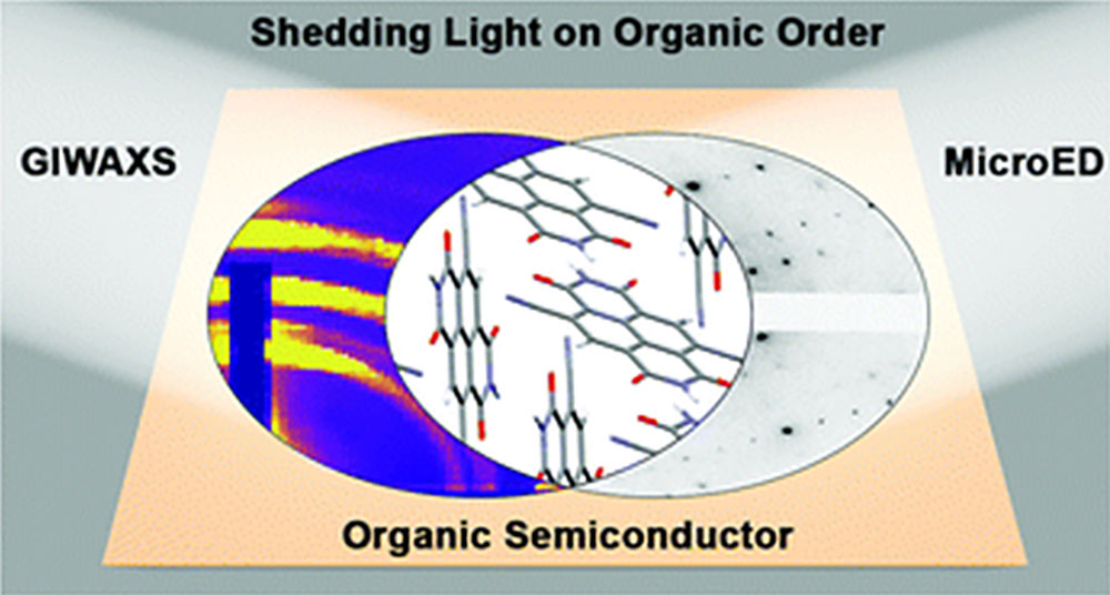
Braunschweig's group uses the complementary characterization techniques of microcrystal electron diffraction (MicroED) and grazing-incidence wide-angle x-ray scattering (GIWAXS) to study the crystal structure and orientation of organic semiconductors in thin films. This information is essential for understanding and ultimately predicting the optoelectronic properties of solar cells and other devices made from these materials.
For these thin-film investigations, Andrew has been performing grazing-incidence wide-angle x-ray scattering (GIWAXS) experiments at NSLS-II’s Soft Matter Interfaces (SMI) beamline with the help of CFN Electronic Nanomaterials Group leader Kevin Yager and staff scientist Esther Tsai. Esther has showed Andrew not only how to perform the measurements but also how to process the data using software developed at the beamline and interpret the results.
Why do you need to combine MicroED and GIWAXS?
We use MicroED to solve the structure of the molecules in nanocrystalline form and GIWAXS to see if the structure is the same in the thin films. GIWAXS also provides information on the crystallinity and orientation of the molecules in the thin films. X-rays hit the thin films at a shallow angle, scattering in a pattern that is unique to how the molecules are packed together.
For our initial study, we looked at three different organic semiconductor compounds. All the compounds are chromophores that absorb light in the visible range and, with modifications of some of the molecules, are industrial dyes such as fire-engine red and Ferrari red. Organic semiconductors are normally insulating, but when they are excited with light or injected with charge, they become conducting. The way that they conduct electrical charge and a lot of their other electronic properties are based on how the molecules are packed.
Combining MicroED and GIWAXS is a really great starting point for design. We can say with confidence that the molecules are packed in a particular way in our films, even if we can’t form large crystals of the material itself. Once we have this information, we can study how charge is transported between molecules and how making modifications to the molecules to affect their packing impacts their optoelectronic properties. For example, we recently synthesized a molecule that has two different crystal structures, or polymorphs. One crystallizes relatively easily; the other one doesn’t. Using MicroED, we can see both structures; with GIWAXS, we can see the relative amounts of the different polymorphs in thin films change as a function of film annealing time. So, we now have a method to control the packing geometry of this molecule in the thin films.
 enlarge
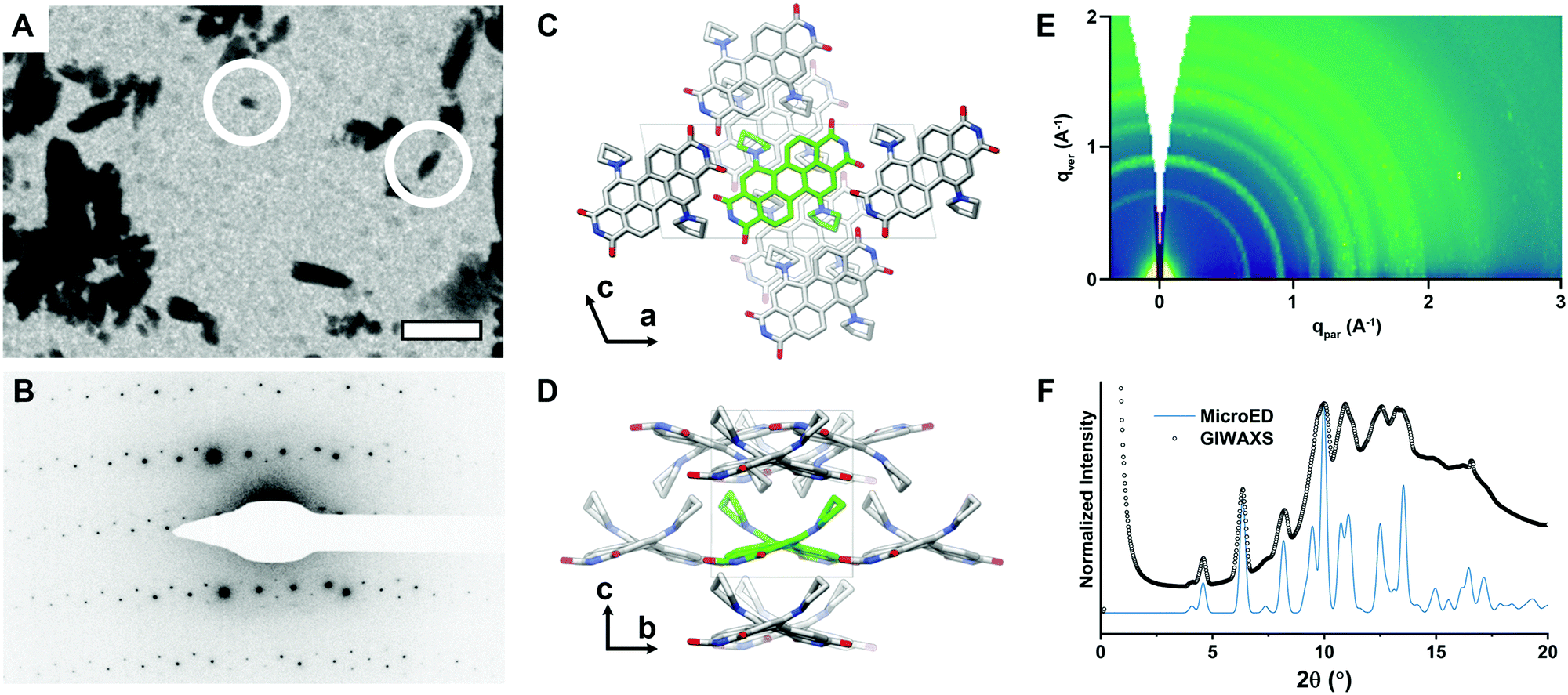
Using a transmission electron microscope, the group imaged nanocrystallites of three organic semiconductor compounds, including dPyr PDI (A), with the circles indicating particles selected for further analysis. The scale bar is two microns. Then, they used MicroED to generate diffraction patterns of the crystallites while rotating the sample; one snapshot is shown in (B). With software, they obtained the crystal structure from these diffraction patterns (C and D). A single molecule is shown in green. At NSLS-II with the help of CFN scientists, they collected GIWAXS measurements on thin films (E). By comparing the MicroED and GIWAXS results, they determined that the crystal structure in the nanocrystallites and thin films is the same (F). This comparison subsequently helped them determine the orientation of molecules in the films. Published in Chem. Commun., 2020, 56, 4204–4207.
Once you’ve determined the structures of the organic semiconductors, how do you correlate these structures with the electronic properties that arise when the materials are exposed to light?
We’re collaborating with colleagues at the ASRC to investigate the optoelectronic properties of the organic semiconductor compounds through spectroscopy and by incorporating them into electronic devices. Actually, one of the spectroscopists in the ASRC Photonics Initiative is former CFN scientist Matthew Sfeir. We hope to start working with him soon to get photophysical data on these materials. Molecules excited with light decay into different excited states, and what we’re interested in whether these states live long enough to be harvested for solar energy applications. Spectroscopy studies will help us make correlations between structure and photophysics that are critical to optimizing device functionality. For example, with the polymorph study, our goal is to show that the two polymorphs have different excited state yields.
Combining the capabilities at the ASRC and Brookhaven Lab, which is only a train ride away, we’ve been able to drive a lot of good science. Seeing our materials progress toward actualization into something useful is very exciting.
The CFN and NSLS-II are both DOE Office of Science User Facilities.
Interested in becoming a CFN user? Submit a proposal through the online proposal system. The next deadline is June 15. If you have questions about the CFN user program or the new CFN Proposal Portal (CPP), please contact CFN User Program Administrator and Outreach Coordinator Grace Webster at (631) 344-3227 or gwebster@bnl.gov. For questions about using CFN facilities or partnering with CFN scientists, please contact CFN Assistant Director for Strategic Partnerships Priscilla Antunez at (631) 344-6186 or pantunez@bnl.gov.
Brookhaven National Laboratory is supported by the U.S. Department of Energy’s Office of Science. The Office of Science is the single largest supporter of basic research in the physical sciences in the United States and is working to address some of the most pressing challenges of our time. For more information, visit https://energy.gov/science.
Follow @BrookhavenLab on Twitter or find us on Facebook.
2020-17233 | INT/EXT | Newsroom