Scientists Build Nanoscale Parapets, Aqueducts, and Other Shapes
Array of novel nanoscale architectures formed through guided self-assembly could yield materials with improved electronic, optical, and mechanical properties
November 17, 2022
 enlarge
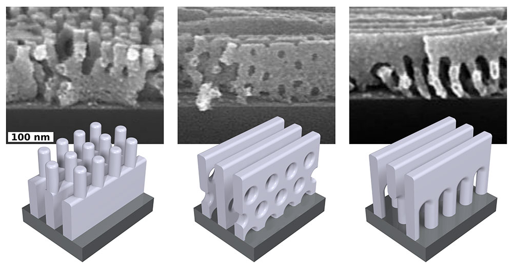
Layering block copolymers and heating them for different times resulted in a range of exotic nanoscale structures (scale bar is 100 nanometers). This image shows scanning electron micrographs and cartoon representations of parapets (cylinders on top and lamellae on bottom), a Swiss-cheese-like patchwork of porous lamellae, and aqueducts (lamellae on top of cylinders). Metals or oxides formed in these shapes could have properties useful for sensors, membranes, transistors, and more.
UPTON, NY—Scientists at the U.S. Department of Energy’s (DOE) Brookhaven National Laboratory have developed a new way to guide the self-assembly of a wide range of novel nanoscale structures using simple polymers as starting materials. Under the electron microscope, these nanometer-scale structures look like tiny Lego building blocks, including parapets for miniature medieval castles and Roman aqueducts. But rather than building fanciful microscopic fiefdoms, the scientists are exploring how these novel shapes might affect a material’s functions.
The team from Brookhaven Lab’s Center for Functional Nanomaterials (CFN) describes their novel approach to control self-assembly in a paper just published in Nature Communications. A preliminary analysis shows that different shapes have dramatically different electrical conductivity. The work could help guide the design of custom surface coatings with tailored optical, electronic, and mechanical properties for use in sensors, batteries, filters, and more.
“This work opens the door to a wide range of possible applications and opportunities for scientists from academia and industry to partner with experts at CFN,” said Kevin Yager, leader of the project and CFN’s Electronic Nanomaterials group. “Scientists interested in studying optical coatings, or electrodes for batteries, or solar cell designs could tell us what properties they need, and we can select just the right structure from our library of exotic shaped materials to meet their needs.”
Automatic assembly
To make the exotic materials, the team relied on two areas of longstanding expertise at CFN. First is the self-assembly of materials called block copolymers—including how various forms of processing affect the organization and rearrangement of these molecules. Second is a method called infiltration synthesis, which replaces rearranged polymer molecules with metals or other materials to make the shapes functional—and easy to visualize in three dimensions using a scanning electron microscope.
 enlarge
Kevin Yager, leader of the Electronic Nanomaterials group at Brookhaven National Laboratory's Center for Functional Nanomaterials (CFN), led this research on a new way to form exotic nanoscale structures by layering block copolymers and exploring the effects of non-equilibrium processing.
“Self-assembly is a really beautiful way to make structures,” Yager said. “You design the molecules, and the molecules spontaneously organize into the desired structure.”
In its simplest form, the process starts by depositing thin films of long chainlike molecules called block copolymers onto a substrate. The two ends of these block copolymers are chemically distinct and want to separate from each other, like oil and water. When you heat these films through a process called annealing, the copolymer’s two ends rearrange to move as far apart as possible while still being connected. This spontaneous reorganization of chains thus creates a new structure with two chemically distinct domains. Scientists then infuse one of the domains with a metal or other substance to make a replica of its shape, and completely burn away the original material. The result: a shaped piece of metal or oxide with dimensions measuring mere billionths of a meter that could be useful for semiconductors, transistors, or sensors.
“It’s a powerful and scalable technique. You can easily cover large areas with these materials,” Yager said. “But the disadvantage is that this process tends to form only simple shapes—flat sheetlike layers called lamellae or nanoscale cylinders.”
Scientists have tried different strategies to go beyond those simple arrangements. Some have experimented with more complex branching polymers. Others have used microfabrication methods to create a substrate with tiny posts or channels that guide where the polymers can go. But making more complex materials and the tools and templates for guiding nano-assembly can be both labor-intensive and expensive.
“What we're trying to show is that there’s an alternative where you can still use simple, cheap starting materials, but get really interesting, exotic structures,” Yager said.
Stacking and quenching
The CFN method relies on depositing block copolymer thin films in layers.
“We take two of the materials that naturally want to form very different structures and literally put them on top of one another,” Yager said. By varying the order and thickness of the layers, their chemical composition, and a range of other variables including annealing times and temperatures, the scientists generated more than a dozen exotic nanoscale structures that haven’t been seen before.
“We discovered that the two materials don’t really want to be stratified. As they anneal, they want to mix,” Yager said. “The mixing is causing more interesting new structures to form.”
If annealing is allowed to progress to completion, the layers will eventually evolve to form a stable structure. But by stopping the annealing process at various times and cooling the material rapidly, quenching it, “you can pull out transient structures and get some other interesting shapes,” Yager said.
Scanning electron microscope images revealed that some structures, like the “parapets” and “aqueducts,” have composite features derived from the order and reconfiguration preferences of the stacked copolymers. Others have crisscross patterns or lamellae with a patchwork of holes that are unlike either of the starting materials’ preferred configurations—or any other self-assembled materials.
Through detailed studies exploring imaginative combinations of existing materials and investigating their “processing history,” the CFN scientists generated a set of design principles that explain and predict what structure is going to form under a certain set of conditions. They used computer-based molecular dynamics simulations to get a deeper understanding of how the molecules behave.
“These simulations let us see where the individual polymer chains are going as they rearrange,” Yager said.
 enlarge
The Center for Functional Nanomaterials (CFN) at Brookhaven National Laboratory provides state-of-the-art capabilities for the fabrication and study of nanoscale materials, with an emphasis on atomic-level tailoring to achieve desired properties and functions.
Promising applications
And, of course, the scientists are thinking about how these unique materials might be useful. A material with holes might work as a membrane for filtration or catalysis; one with parapet-like pillars on top could potentially be a sensor because of its large surface area and electronic connectivity, Yager suggested.
The first tests, included in the Nature Communications paper, focused on electrical conductivity. After forming an array of newly shaped polymers, the team used infiltration synthesis to replace one of the newly shaped domains with zinc oxide. When they measured the electrical conductivity of differently shaped zinc oxide nanostructures, they found huge differences.
“It’s the same starting molecules, and we’re converting them all into zinc oxide. The only difference between one and the other is how they’re locally connected to each other at the nanoscale,” Yager said. “And that turns out to make a huge difference in the final material’s electrical properties. In a sensor or an electrode for a battery, that would be very important.”
The scientists are now exploring the different shapes’ mechanical properties.
“The next frontier is multifunctionality,” Yager said. “Now that we have access to these nice structures, how can we choose one that maximizes one property and minimizes another—or maximizes both or minimizes both, if that’s what we want.”
“With this approach, we have a lot of control,” Yager said. “We can control what the structure is (using this newly developed method), and also what material it is made of (using our infiltration synthesis expertise). We look forward to working with CFN users on where this approach can lead.”
This research was funded by the DOE Office of Science (BES). The experimental work was led by Sebastian Russell, a postdoctoral fellow at the CFN who is now working in industry. Additional co-authors include Masafumi Fukuto of Brookhaven Lab’s National Synchrotron Light Source II (NSLS-II); Chang-Yong Nam, Suwon Bae, Nikhil Tiwale, and Gregory Doerk of CFN; and Ashwanth Subramanian of Stony Brook University (SBU). CFN and NSLS-II are DOE Office of Science User Facilities. This work also used computational resources managed by the Scientific Data and Computing Center, a component of the Computational Science Initiative at Brookhaven Lab.
Brookhaven National Laboratory is supported by the Office of Science of the U.S. Department of Energy. The Office of Science is the single largest supporter of basic research in the physical sciences in the United States and is working to address some of the most pressing challenges of our time. For more information, visit science.energy.gov.
Follow @BrookhavenLab on Twitter or find us on Facebook.
2022-20932 | INT/EXT | Newsroom


