Peering into Functioning Batteries with Sooyeon Hwang
interview with a CFN staff member
May 21, 2020
 enlarge
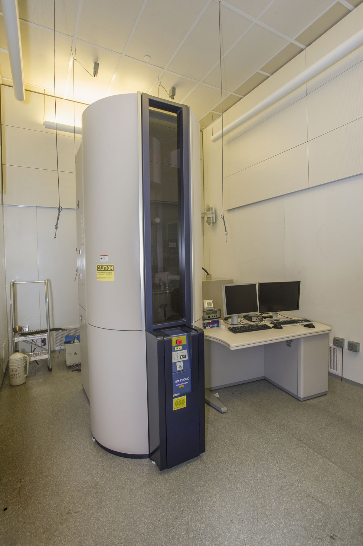
Materials scientist Sooyeon Hwang in the Electron Microscopy Facility at Brookhaven Lab's Center for Functional Nanomaterials. On her computer screens are elemental maps she acquired using the characterization techniques of energy-dispersive x-ray spectroscopy and scanning transmission electron microscopy. These maps show the distribution of chemical elements in qubit samples. Qubits are made of "objects" such as atoms, ions, photons of light, or electrons whose quantum states can be accessed and controlled optically, magnetically, or by other means.
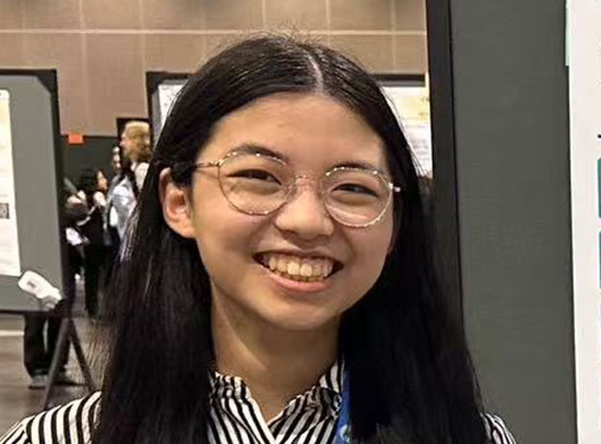
Sooyeon Hwang is a staff scientist in the Electron Microscopy Group at the Center for Functional Nanomaterials (CFN)—a U.S. Department of Energy (DOE) Office of Science User Facility at Brookhaven National Laboratory. Here, she uses state-of-the-art transmission electron microscopes (TEMs) to characterize the structural and chemical dynamics of electrode (cathode and anode) materials during battery operation. Through her research, she aims to improve the performance of batteries by acquiring fundamental knowledge about how these energy-storage materials react and degrade at the nanoscale. Hwang holds three degrees in materials science and engineering: a BS from Ajou University, and an MS and a PhD from the Korea Advanced Institute of Science and Technology (KAIST), both institutions in her native South Korea.
You grew up and completed your education in South Korea. When did you first come to the United States, and what led you to the CFN?
During undergrad, I spent one semester at the University of Florida. I’ve had somewhat of a long connection with the CFN. During my PhD, I conducted research at the CFN through the Global Research Laboratory program, which promotes collaborative research between Korean and foreign institutions. At the time, there was a collaboration between senior members of the Korea Institute of Science and Technology (KIST) and Brookhaven Lab staff, including Eric Stach—then-leader of the CFN Electron Microscopy Group.
 enlarge
A series of (a) transmission electron microscope (TEM) images, (b) TEM diffraction patterns, and (c–e) electron energy-loss spectra demonstrating the thermal degradation of cathode materials made of lithium (Li), nickel (Ni), cobalt (Co), aluminum (Al), and oxygen (O) (LixNi0.8Co0.15Al0.05O2, referred to as NCA) during heating at high temperatures. Published in ACS Appl. Mater. Interfaces 6, 15140 (2014).
The microscopes I was using in South Korea were very old, with only imaging and diffraction capabilities. The CFN has much more advanced microscopes than the ones I had access to. For example, the CFN has TEMs with spherical aberration correctors, which enable ultrahigh image resolution, and in situ sample holders for dynamic experiments. I used these capabilities to study the thermal stability of cathode materials in lithium (Li)-ion batteries. After cycling small single-cell batteries called coin cells, I increased the temperature inside the TEM to see how the crystal structure and chemical properties of the cathode particles changed. I discovered that after cycling, the thermal stability degrades as more Li is extracted.
After spending one and a half years at the CFN, I went back to South Korea to finish my PhD. Then I did a one-year postdoc at the KIST Center for Energy Convergence. In 2016, I heard that the CFN Electron Microscopy Group was hiring a postdoc. I applied and was offered the position. For my postdoc at the CFN, I continued my research on electrode materials for Li-ion batteries, working with electron microscopist Dong Su, who ended up becoming the leader of the group. Three years later, I was promoted to CFN Staff Scientist.
Having access to the instruments you need for your research is one thing, but knowing how to operate those instruments is another. How did you get up to speed on the capabilities of the CFN TEMs while you were a PhD student?
I acquired fundamental knowledge about electron microscopes through my coursework, and Eric was a critical resource during my PhD studies. When I first arrived, Eric said to me, “What can I do for you?” His welcoming and willingness to help was a culture shock to me. In South Korea, the principal investigators generally tell you what to do. Eric not only helped me with my project but also guided me as a microscopist. From him, I learned how to perform various in situ techniques, correct the electron beam, and analyze TEM images and diffraction patterns.
Because I wasn’t familiar with some of the science terminology and the fundamentals behind the techniques, I had to overcome a big learning curve. During this time, I studied a lot. I felt a little uncomfortable and nervous because I wasn’t publishing at all, and PhD students are expected to author a lot of papers. But I think it ended up being a very productive period for me. I went back to South Korea able to write a number of papers based on experiments that I had conducted at the CFN.
Besides the culture shock and learning curve you experienced when you arrived at the CFN, what else marked your transition? Did you encounter other challenges, such as language barriers?
I had English classes starting in middle school. And, in undergrad, we actually learn science with textbooks written in English. But language is definitely a big barrier. Sometimes I forget the words I am looking for or am unsure if I have understood a particular expression correctly. Having leaders and colleagues whom I can turn toward to ask questions has made my transition much easier.
In a way, each scientist speaks his or her own language in terms of scientific expertise and specialty. By bringing this knowledge together, we can build a complete picture of a material. For example, for one of my research projects, I performed electron microscopy studies of single-atom nickel (Ni) catalysts while coworkers synthesized the materials, tested their catalytic properties, and analyzed them with different characterization tools, such as x-ray absorption spectroscopy. Because of these collaborations, I have been publishing a lot more. Since joining the CFN in 2016, I have published about 40 papers in peer-reviewed journals, including Nature and its sister journals. This aspect of working at the CFN is something that I often think about because my success as a scientist is partly determined by the number of publications I author and their scientific impact.
Since joining the CFN, you’ve focused your research on cathode and anode materials. What are some of the projects you’re currently working on?
 enlarge
Sooyeon Hwang (sitting), Dong Su (left, standing), and Shuang Li used electron microscopes to see how the crystal structure and chemical nature of a battery electrode material made of an iron-oxide (magnetite) evolved as lithium was inserted and extracted over 100 charge and discharge cycles. CFN Research Highlight. Note: This photo was taken prior to current COVID-19 social distancing guidelines.
On the anode materials side, I’m studying conversion reactions with iron (Fe) or Ni oxide of different stoichiometries. After lithiation, when Li is extracted, the structure of the anode materials is completely different from that of the pristine (original) state. I’m trying to understand what the structural and chemical differences are after one cycle and how these differences affect the electrochemical properties of the material. Unlike the several stable oxidation states of Fe oxide—for example, Fe2O3 and Fe3O4—Ni oxide is only stable with a +2 oxidation state. Because of these different stoichiometries, comparing Ni and Fe oxides is very interesting. One of the key results from these studies so far is that the conversion reaction is not reversible in Fe oxide. Regardless of the stoichiometry, the original composition is not completely restored. This irreversibility could be a route for battery capacity fade.
For my second project, I’m studying the solid-solid interface between Li-rich cathode materials and a solid electrolyte called LiPON (lithium phosphorous oxynitride) during Li extraction and insertion. All-solid-state Li-ion batteries are a kind of next-generation Li-ion battery. Conventionally, Li-ion batteries use liquid electrolytes, which are flammable. Because of this safety issue, the battery community is looking to replace the liquid electrolytes with safer materials. Solid electrolytes are one of the alternative options.
 enlarge
The in situ lithiation of epitaxial iron oxide (Fe3O4) thin films on a niobium (Nb)-doped strontium titanate (SrTiO3) substrate revealed that compressive strain originating from lattice mismatch delays the lithiation reaction near the interface between the thin film and substrate. (a) An image showing the experimental setup. (b) A high-angle annular dark-field scanning TEM image showing the atomic structure. (c) An atomic model at the interface. (d) A schematic of the experimental details. (e) A series of images showing Li diffusion. (f) Simulated Li diffusion over time. Published in Agnew. Chem. Int. Ed. 129, 7921–7924 (2017).
What TEMs are available at the CFN, and how are you applying them to study these battery materials?
The CFN has five TEMs: one manufactured by Hitachi, which I manage; two by JEOL; and two by FEI Company, which is part of Thermo Fisher Scientific. Each microscope has different capabilities and specialties, and each vendor has its own kind of sample holders. Luckily, the CFN has various in situ holders that can be adapted to fit different microscopes. I take advantage of electrical biasing holders for in situ lithiation experiments.
Generally, with TEM, I do imaging, diffraction, and chemical analysis. Imaging tells you the morphology and size of your samples. At high magnification, you can perform atomic-resolution imaging to see how the atoms are arranged. The diffraction patterns produced when the electron beam interacts with the sample are mostly for structural analysis. And for chemical analysis, I use two techniques: electron energy-loss spectroscopy (EELS), which detects scattered electrons from a sample, and energy-dispersive x-ray spectroscopy (EDX), which detects x-rays emitted from a sample. Together with a scanning electron beam, EELS and EDX provide localized chemical information, such as chemical bonds, chemical composition, and oxidation states.
 enlarge
The Hitachi microscope at the CFN is ideal for probing the structural and electronic properties of materials at the angstrom (one hundred-millionth of a centimeter) level.
You mentioned that you manage the Hitachi microscope. What does management of this instrument entail?
In addition to making sure that the microscope is functioning as it should be, I train users on how to use the microscope and help them operate it. If there is an issue with the microscope—for example, recently, one of the pumps wasn’t working properly—I am responsible for addressing it. I also perform general upkeep on a monthly basis. This maintenance includes aligning the beam and “baking,” or applying heat to remove gases and other contaminants from the column. Another one of my tasks is keeping the microscope state of the art. In the near future, the EELS system will be upgraded. I am excited about this upgrade because we will get sharper spectra over shorter timescales.
Interacting with users of the microscope, you must get exposed to different disciplines. How have these interactions impacted your own research?
Yes, that is one of the great points of interacting with the users of the microscope—I’ve gained lots of experience helping them research various materials. Since May 2019, I have worked with about 20 different groups of CFN users, who are studying batteries, catalysts, superconductors, qubits, and solar cells, to name a few. Even though I am usually not an expert in the field my users work in, I nonetheless learn new things. It’s exciting to leverage my expertise to help them better understand their materials.
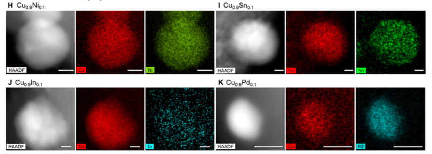
For example, I recently collaborated with a group led by the University of Maryland, College Park, to characterize nanoparticles synthesized from two different metallic components. These bimetallic systems are of interest for catalysis because they often have unique chemical properties relative to the single metals. However, in many bimetallic systems, the metals do not evenly mix because of thermodynamics. In this research, the team implemented a kinetics-based method to make homogenous bimetallic nanoparticles. Analysis via scanning TEM (STEM) and EDX were critical in visualizing the atomic arrangement of the bimetallics and the chemical distribution of each element in single nanoparticles. By overcoming thermodynamic rules, we have more opportunities to design and synthesize materials with optimal catalytic properties.
 enlarge
Via conventional bimetallic synthesis, metals such as nickel (Ni), tin (Sn), indium (In), and palladium (Pd) do not mix uniformly with copper (Cu). The new method overcomes this thermodynamic immiscibility, as seen in the electron microscope images and corresponding elemental maps above. Recently published in Science Advances, vol. 6, no. 17 (2020).
Another great aspect about working with users is that sometimes their expertise from a completely different discipline helps me with my own research. Even knowledge from within the same general field can be impactful. For example, I was helping a battery researcher studying different solid electrolytes, and because of our discussions on Li-rich cathode materials, I decided to try LiPON as a solid electrolyte in my own research.
Users are one source of fresh perspectives; staff—whether at the CFN or across Brookhaven Lab—are another. Are you collaborating with any staff?
At the CFN, I’m starting to collaborate with colleagues to realize systems inside the TEM to see atomic motion during the extraction of 2-D materials and to obtain electrochemical measurements. Outside of the CFN, I’ve been consulting with members of the Electrochemical Energy Storage Group in Brookhaven’s Chemistry Division for battery testing. With the help of beamline scientists, I’ve been conducting complementary experiments at the Pair Distribution Function (PDF) beamline of the National Synchrotron Light Source II (NSLS-II) [another DOE Office of Science User Facility at Brookhaven]. TEM observations are very localized, whereas PDF provides averaged structural information, especially at short-range order from a large sample area. Thus, combining the two techniques can provide a more complete understanding of battery material structures.
How did you come to specialize in electron microscopy–based battery research? When did you start thinking about pursuing a science career?
High school in South Korea is typically for three years, and during the first year, you need to choose whether you’re going to focus on science or liberal arts for the remaining two years. When I told my mom I’d be picking science, she was surprised. She expected me to be a reporter or do some other media-related profession. But at that time, I liked math and science more because it was less ambiguous than liberal arts. Writing and solving equations were much clearer to me.
Once I made the decision to do science, I read a lot about different fields of science to find out what each involved. When I came upon materials science and engineering, I thought it would be a good fit in terms of my interests in fundamental science and practical applications. Materials science and engineering is kind of a balance between general science and engineering.
Right after I entered grad school, I figured I should choose what to do for both my master’s degree and PhD. I was interested in electron microscopy because I thought it was fascinating to see the atomic arrangements of materials. At the time, I didn’t know I’d eventually be training and helping others extract scientific meaning from these images.
The research group I joined at grad school focused on electron microscopy, and most of the group members studied well-crystallized thin-film oxides for semiconductor display applications. I wanted to do something different, and my PhD advisor recommended that I explore battery materials with scientists at KIST. Back then, electron microscopy was being applied in the battery field on a very limited level. The possibility of discovering something new from electrode materials with electron microscopes was exciting to me.
What do you hope to achieve as a member of the battery science community?
In the long term, I want to be widely known as an electron microscopist specializing in battery research. One of my short-term goals is to be an invited speaker at a conference. In general, conferences are meetings for very specific research areas, and an invitation to speak would help increase my recognition as an independent scientist. Moreover, because my research leverages both battery science and electron microscopy, I would like to write review papers that can help electron microscopists find opportunities to apply their work to battery science and battery scientists to analyze their materials by electron microscopy. For example, last year, I co-authored a review about an in situ analysis technique for studying cathode materials.
I’m also very interested in engaging with industry researchers to answer more applied questions, such as the causes of device failure. When a device malfunctions, the structure and chemistry of the materials inside may be changed. I can investigate these changes with electron microscopy techniques. Partnering with industry would also be beneficial to my own research because industry has a deeper understanding of devices operating in the real world. For instance, my discussions with industry researchers at a meeting of the Korean Electrochemical Society in 2014 provided new perspectives on the materials that I work on. At this meeting, I had the chance to chat with a researcher from LG Chem about my research on cathode materials. He was interested in my electron microscopy studies of charge-induced (lithium extraction) structural evolutions and suggested that I explore the effect of discharge (lithium insertion) on microstructures, as charge and discharge are both important in battery operation.
I was thrilled to participate as a reviewer for the 2020 DOE Small Business Innovation Research (SBIR) Program, which helps small businesses conduct research and development (R&D) projects with the potential for commercialization. I evaluated and provided feedback to businesses that submitted proposals to meet DOE mission-specific R&D needs. My experience as a reviewer was a good opportunity to learn how science activities can be expanded into a business. It also got me to start brainstorming business ideas regarding electron microscope advances that can enable scientists to perform in situ experiments more easily or realize completely new kinds of experiments. Having this kind of impact would be a significant achievement in my scientific career.
Brookhaven National Laboratory is supported by the Office of Science of the U.S. Department of Energy. The Office of Science is the single largest supporter of basic research in the physical sciences in the United States and is working to address some of the most pressing challenges of our time. For more information, please visit https://www.energy.gov/science.
Follow @BrookhavenLab on Twitter or find us on Facebook.
2020-17232 | INT/EXT | Newsroom