
CD-0
The Center for Functional Nanomaterials (CFN) is granted Critical Decision 0 (CD-0) by the U.S. Department of Energy (DOE), the first of what would prove to be many milestones.
First Users (Jumpstart)
The CFN's User program gets its early beginnings with the Jumpstart program: using existing Brookhaven Lab facilities to do nanoscience and to build the foundation of a growing user base.
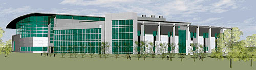
CD-1
The next milestone for the CFN kicked off the project and design of the new facility.
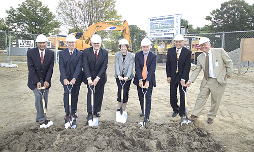
Groundbreaking
Construction of the CFN begins.
Mendez Begins as Director
Emilio Mendez, a former IBM scientist and Stony Brook University professor, begins his tenure as the first director of the CFN. More...
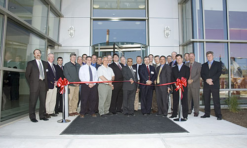
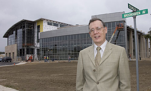
Ribbon Cutting
Completion of the CFN building is marked by a ribbon-cutting ceremony.
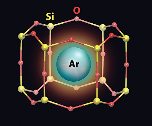
AP-XPS 1st Pub
One of the top 10 accomplishments of the CFN's first 10 years: CFN researchers enable atomic-scale understanding of catalytic processes enabled by in situ ambient-pressure x-ray photoelectron spectroscopy (AP-XPS) at the National Synchrotron Light Source (NSLS)—and now NSLS-II.
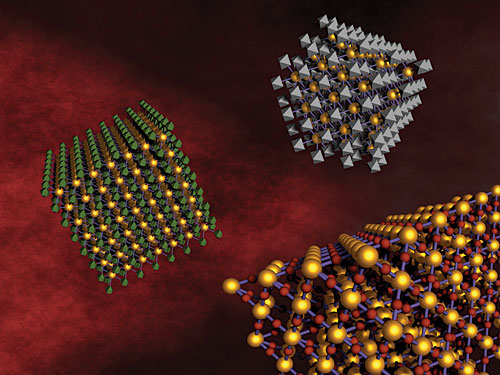
1st Publication of DNA Accomplishment
One of the top 10 accomplishments of the CFN's first 10 years: Oleg Gang and his group first report DNA-programmable, self-assembled nanoparticle architectures. More...
Open for Operations
The CFN is officially open for business as operations begin in spring 2008.
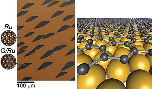
1st Publication of Graphene Growth Accomplishment
One of the top 10 accomplishments of the CFN's first 10 years: in a highly cited Nature Materials paper published in 2008, Peter Sutter and Eli Sutter first report their results on the synthesis and characterization of graphene grown on transition-metal substrates.
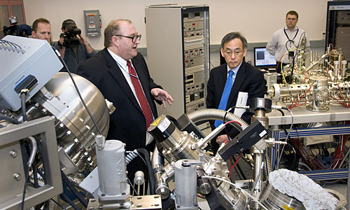
Energy Secretary Chu Visits
The CFN hosts thousands of visitors in its first 10 years, from politicians to high-school students. In 2009, Secretary of Energy Steven Chu visits and tours the facility.
U.S. Senator Gillibrand Visits
The CFN hosts thousands of visitors in its first 10 years, from politicians to high school students. Also in 2009, the CFN hosts New York Senator Kirsten Gillibrand.
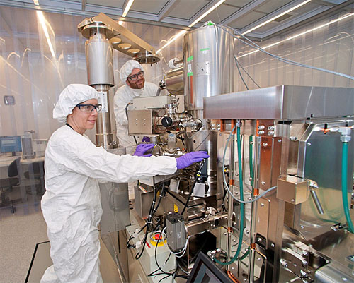
JEOL JBX-6300FS E-Beam Writer Installed
In June 2009, a state-of-the-art electron-beam lithography instrument is installed in the CFN nanofabrication facility, quickly becoming one of the highest-subscribed instruments at the facility and leading to many high-impact user publications.
Nanoscale Junctions
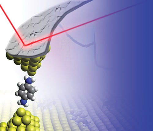
One of the top 10 accomplishments of the CFN's first 10 years: Mark Hybertsen and CFN User Lena Venkataraman publish their first result on electronic and mechanical structure-function relationships in nanoscale junctions. The work has received more than 1,900 citations to date.
Single-digit EBL
One of the top 10 accomplishments of the CFN's first 10 years: a collaboration between MIT and CFN scientists using the scanning tunneling electron microscope as a patterning tool leads to record-breaking single-digit electron beam lithography (EBL).
X-ray Scattering for Nanoscience
One of the top 10 accomplishments of the CFN's first 10 years: Kevin Yager, working in partnership with NSLS and NSLS-II, develops premier x-ray scattering beamlines for nanoscience, leading to more than 135 publications to date.
Operando TEM Facility
One of the top 10 accomplishments of the CFN's first 10 years: Eric Stach and the Electron Microscopy group staff develop a transmission electron microscopy (TEM) facility designed specifically for in situ and operando studies of nanomaterials.
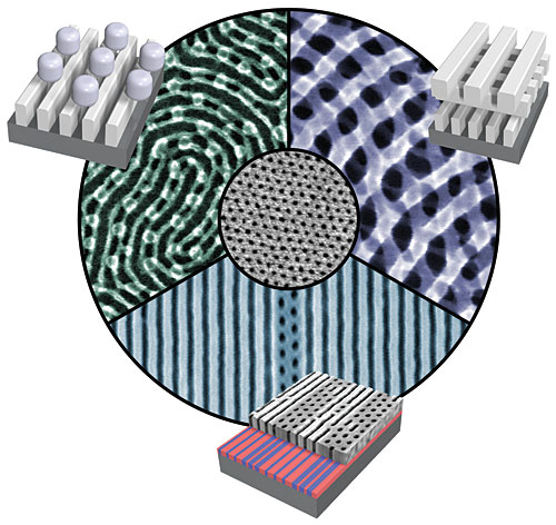
1st Publication of Block Copolymer Accomplishment
One of the top 10 accomplishments of the CFN's first 10 years: Chuck Black and collaborators advance the use of block copolymer self-assembly for the design and fabrication of high-performance surface nanostructures.
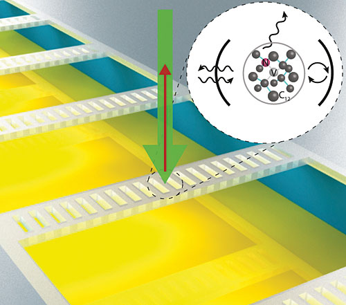
Diamond Pub
One of the top 10 accomplishments of the CFN's first 10 years: CFN User Dirk Englund, working in collaboration with CFN staff, develop sophisticated nanofabrication processes for building high-quality photonic structures in diamond.
The first partner CFN/NSLS-II instrument comes online: Ambient Pressure Photoelectron Spectroscopy
CFN and NSLS-II staff have worked together to develop and jointly operate four partner instruments. The first of these, ambient-pressure photoelectron spectroscopy, uses X-rays to follow chemical changes on surfaces at realistic conditions.
Publication of Singlet Fission
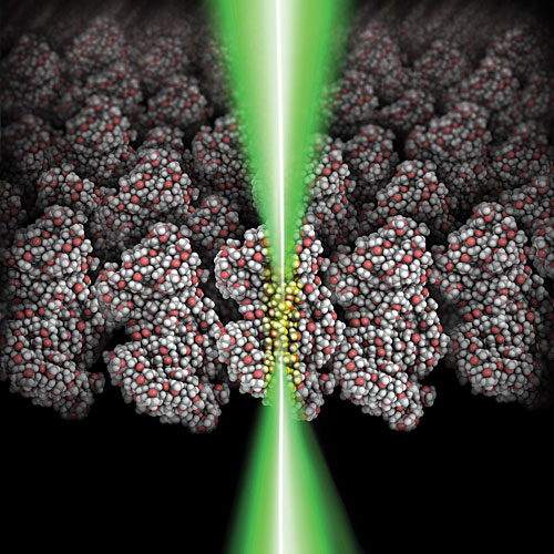
One of the top 10 accomplishments of the CFN's first 10 years: Matt Sfeir and CFN User Luis Campos at Columbia University demonstrate the first example of an isolated-molecule singlet-fission material.
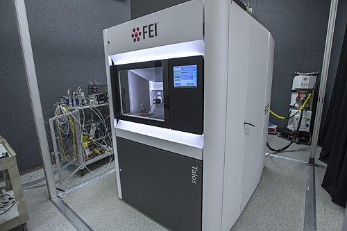
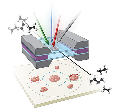
Operando Scanning Transmission Electroscope Available to CFN Users
The CFN’s cutting-edge electron microscopy facility adds the new FEI Talos microscope, expanding department’s capability on imaging materials at the nanoscale in-operando: operating in real-world conditions.
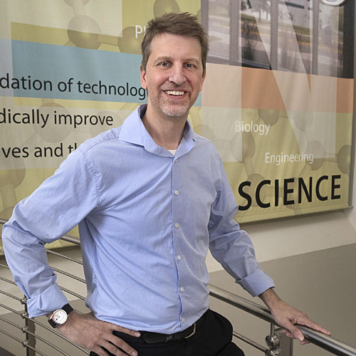
Black Takes the Helm
Taking over for Emilio Mendez, Electronic Materials group leader Charles Black becomes the second CFN director. More...
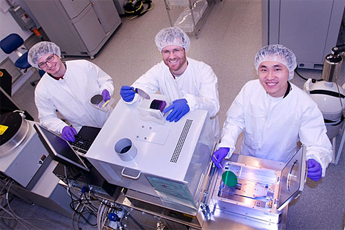
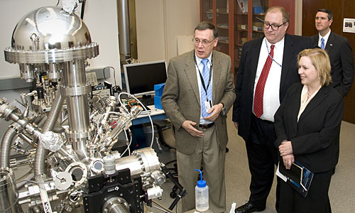
Visit from Secretary of Energy Rick Perry
Secretary of Energy Rick Perry and Congressman Lee Zeldin visit the CFN and get a hands-on tour of the cleanroom.
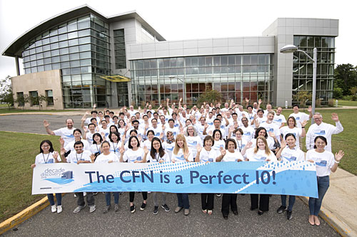
CFN celebrates its first Decade of Discovery!
The Center for Functional Nanomaterials served almost 2500 Users from 44 states and 23 countries in its first ten years. Be a part of our next decade of discovery! More...