Next-Gen Semiconductor Manufacturing Tech Wins DOE National Pitch Competition
Developed at the Center for Functional Nanomaterials, the technology for synthesizing hybrid organic-inorganic materials sensitive to extreme-ultraviolet light could help shrink the size of features on computer chips to boost their speed and energy efficiency
November 1, 2021
 enlarge
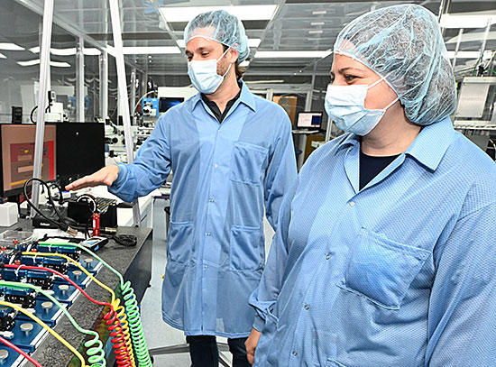
Chang-Yong Nam of the Center for Functional Nanomaterials is the technical lead and inventor of a vapor-based process technology for next-generation semiconductor manufacturing by extreme-ultraviolet lithography—an emerging technique to make computer chips on smaller scales than ever before.
UPTON, NY—A process for making hybrid organic-inorganic materials (photoresists) sensitive to extreme-ultraviolet (EUV) light is one of two technologies that won the 2021 National Labs Accelerator Pitch Event. This technology—developed at the Center for Functional Nanomaterials (CFN), a U.S. Department of Energy (DOE) Office of Science User Facility at Brookhaven National Laboratory—could be used for next-generation semiconductor manufacturing by EUV lithography.
Organized by DOE’s Lawrence Livermore National Laboratory in partnership with the DOE Office of Technology Transitions (OTT) and presented by the UC Davis Institute for Innovation and Entrepreneurship, the National Labs Accelerator Pitch Event accelerates the transfer of new technologies developed at DOE national labs to the private sector. In a Shark Tank-like competition format, lab scientists pitch their technology ideas to a panel of investor and entrepreneur judges. A live question-and-answer session follows these pre-recorded presentations. The judges evaluate the commercial potential of each idea.
For the 2021 event, materials scientist Chang-Yong Nam of the CFN Electronic Nanomaterials Group pitched the photoresist process technology. Nam has been developing this technology for the past three years, with contributions from CFN scientific associate Nikhil Tiwale.
To prepare for the pitch, Nam participated in an entrepreneurial training workshop, a hands-on session for developing an investor pitch deck, and a local pitch competition. These activities are developed and implemented by Brookhaven Lab’s Office of Technology Transfer within the Strategic Partnerships Program Office.
Preparing scientists to move ideas from lab to market
Since 2017, Brookhaven’s Office of Technology Transfer—with grant awards from DOE OTT—has developed and hosted four entrepreneurial workshops. The workshops help scientists identify, understand, and overcome barriers to technology commercialization. To date, more than 75 scientists across the Lab have participated. Scientists are equipped with the skills to explain what their technology is, define value propositions, validate core business assumptions through customer discovery, and work through product renditions. Participants also learn about other commercialization-related opportunities, including OTT’s Technology Commercialization Fund and two-month entrepreneurial training program Energy I-Corps.
After the workshop, scientists who seek to further strengthen their ideas can participate in an intensive customer discovery and pitch development training session. During this session, they develop an investor pitch deck. They learn how to communicate their idea in layman’s terms and convey its importance to investors and potential licensees.
Participants can then compete in a local pitch event judged by workshop alumni. This year, Nam was the finalist; Med Boukhicha of Brookhaven’s Nonproliferation and National Security Department—who developed a novel neutron detector—was the semifinalist.
Following this local pitch event, workshop alumni judges nominate one participant to represent Brookhaven at the national DOE pitch competition. For this year’s event, they selected Nam to pitch his hybrid resist process technology for extreme UV lithography. The other Brookhaven team members who contributed to preparing the pitch are Mingyuan Ge, an associate physicist at the National Synchrotron Light Source II (NSLS-II), another DOE Office of Science User Facility at Brookhaven; Poornima Upadhya, manager of technology transfer; and Yifan Fang, technology transfer intern and PhD candidate at Stony Brook University.
 enlarge
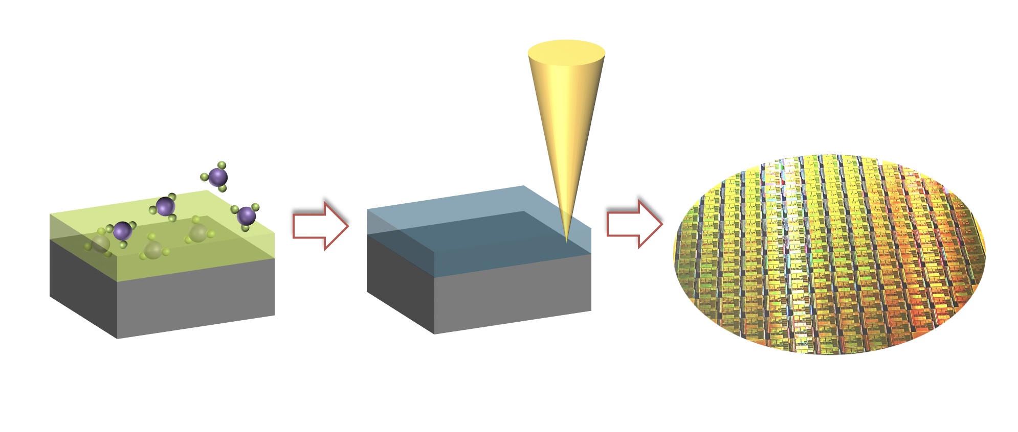
Nam's technology is based on infusing inorganic elements (purple molecules) by vapor into an organic extreme-ultraviolet (EUV) photoresist (green) on a substrate such as silicon (Si). The resulting organic-inorganic hybrid EUV photoresist (blue, middle) can be exposed to EUV light (yellow cone) to pattern next-generation semiconductor devices with reduced dimensions (right).
Extreme lithography for extreme downscaling of device feature sizes
In lithography, light is used to print tiny patterns on transistors, the circuit elements of modern electronics. Scientists begin the process by applying a thin film—conventionally made of an organic material—on a silicon wafer. Then, they shine light of a specific wavelength through a photomask with the desired design.
With current state-of-the-art EUV technology, feature sizes can range from five to ten nanometers, or billionths of a meter. Going below these dimensions will improve the performance and energy efficiency of electronic devices. However, reducing feature sizes comes with several technical challenges. One of these challenges is related to the photoresist.
“Carbon—the main element of the organic photoresists we currently use for EUV lithography—has a very low sensitivity to EUV light,” explained Nam. “Because of this sensitivity, we need to expose the resists to EUV light for a long time. This long exposure time limits the number of wafers we can process per hour.”
Another limitation of organic photoresists for EUV lithography is their poor etch resistance. The resists can degrade as the patterns are etched into silicon. Because of this degradation, patterns with a high height-to-width aspect ratio—needed to make electronic devices—require complex steps to produce.
Here’s where Nam’s patent-pending technology can provide a solution. Through vapor processing, inorganic elements like zinc or tin—which have a high EUV sensitivity and etch resistance—are infused into existing organic photoresists. The chemical composition of the inorganic component can be easily controlled without complex chemical synthesis. Such control is important to modifying and optimizing resist performance on demand to meet manufacturing requirements.
Nam and his team are now looking for industry partners to commercialize the technology. By 2030, the EUV photoresist industry is projected to be worth $1 billion.
“We seek to mature the technology in terms of technical specifications like sensitivity, resolution, and defectivity as per manufacturing requirements and license it to semiconductor manufacturers,” said Nam. “Several semiconductor companies have confirmed the critical market need and expressed interest in our technology.”
The other winner of the 2021 National Labs Accelerator Pitch Event is Brooke Harmon of Sandia National Laboratories for a “Platform for Discovery, Design, and Engineering of Antibody Therapeutics for Emerging Viruses.”
If you are interested in learning about the entrepreneurship training and technology commercialization, contact Brookhaven Office of Technology Transfer Manager Poorni Upadhya at pupadhya@bnl.gov. For more information on how to partner with the CFN, contact CFN Assistant Director for Strategic Partnerships Priscilla Antunez at pantunez@bnl.gov.
Brookhaven National Laboratory is supported by the U.S. Department of Energy’s Office of Science. The Office of Science is the single largest supporter of basic research in the physical sciences in the United States and is working to address some of the most pressing challenges of our time. For more information, visit https://energy.gov/science.
Follow @BrookhavenLab on Twitter or find us on Facebook.
2021-19177 | INT/EXT | Newsroom