Hacking DNA to Make Next-Gen Materials
Scientists developed a universal method for producing a wide variety of functional, 3D metallic and semiconductor nanostructures
January 24, 2024
 enlarge
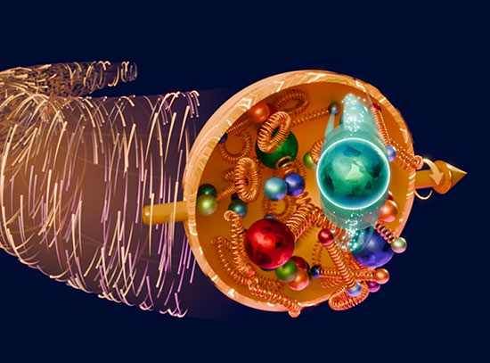
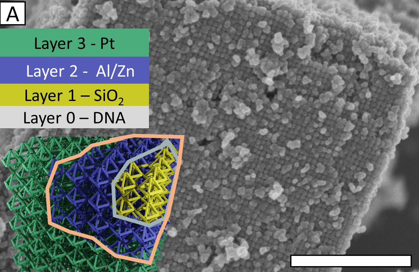
Scientists used a new, universal method to create a variety of 3D metallic and semiconductor nanostructures, including this structure revealed by an electron microscope. The scale bar represents one micrometer. The superimposed graphics convey that the researchers combined multiple techniques to layer silicon dioxide, then alumina-doped zinc oxide, and finally platinum on top of a DNA "scaffolding." This complex structure represents new possibilities for advanced manufacturing at small scales. (Brookhaven National Laboratory)
UPTON, NY—Scientists at the U.S. Department of Energy’s (DOE) Brookhaven National Laboratory, Columbia University, and Stony Brook University have developed a universal method for producing a wide variety of designed metallic and semiconductor 3D nanostructures—the potential base materials for next-generation semiconductor devices, neuromorphic computing, and advanced energy applications. The new method, which uses a “hacked” form of DNA that instructs molecules to organize themselves into targeted 3D patterns, is the first of its kind to produce robust nanostructures from multiple material classes. The study was recently published in Science Advances.
“We have been using DNA to program nanoscale materials for more than a decade,” said corresponding author Oleg Gang, a professor of chemical engineering and of applied physics and materials science at Columbia Engineering and leader of the Soft and Bio Nanomaterials Group at the Center for Functional Nanomaterials (CFN). CFN is a DOE Office of Science user facility at Brookhaven Lab. “Now, by building on previous achievements, we have developed a method for converting these DNA-based structures into many types of functional inorganic 3D nano-architectures, and this opens tremendous opportunities for 3D nanoscale manufacturing.”
Self-Assembly Is in This Team’s DNA
CFN is a leader in researching self-assembly, the process by which molecules spontaneously organize themselves. In particular, scientists at CFN are experts at DNA-directed assembly. Researchers program strands of DNA to “direct” the self-assembly process towards molecular arrangements that give rise to beneficial properties, such as electrical conductivity, photosensitivity, and magnetism. Then, those structures can be scaled up to functional materials. To date, CFN has used DNA-directed assembly to produce switchable thin films, 3D nanosuperconductors, and more.
“We have demonstrated various types of structures we can organize using DNA-directed assembly. But, to take this research to the next level, we can’t only rely on DNA,” Gang said. “We needed to expand upon our method to make more robust structures with more specific functionality for advanced technologies like microelectronics and semiconductor devices.”
Recently, Gang and colleagues, including several students, were able to grow silica, an oxidized form of silicon, onto a DNA lattice. The addition of silica created a much more robust structure, but the procedure was not widely applicable to different materials. The team still needed further research to develop a method that could produce metallic and semiconductor materials in an efficient way.
 enlarge
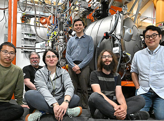
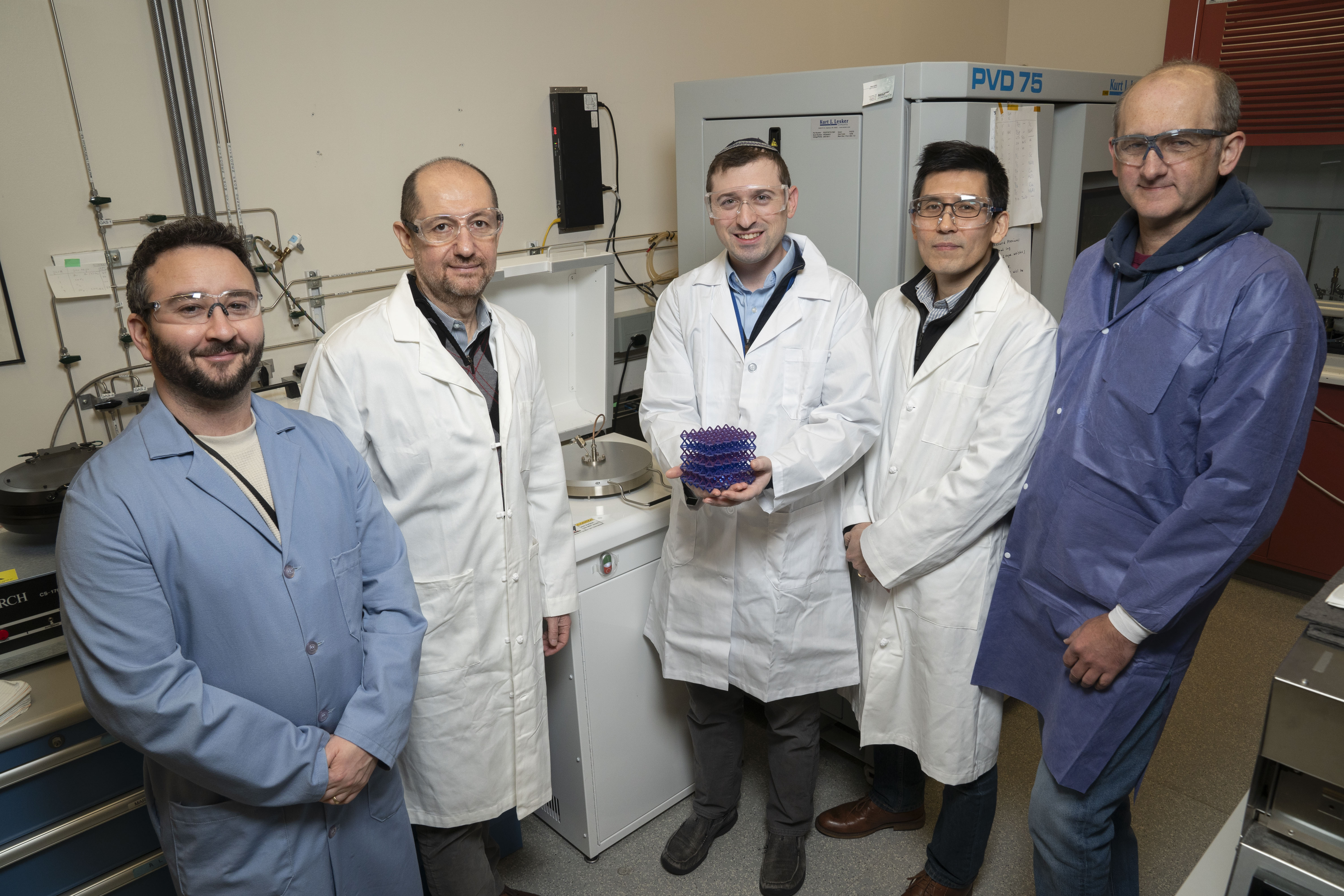
Members of the research team are pictured at the Center for Functional Nanomaterials with a 3D-printed replica of one of their nanostructures. Pictured from left to right are Jason Kahn, Oleg Gang, Aaron Michelson, Chang-Yong Nam, and Dmytro Nykypanchuk. (Jessica Rotkiewicz/Brookhaven National Laboratory)
Stacking Techniques (and Expertise)
To build out a more universal method for producing 3D nanostructures, researchers in CFN’s Soft and Bio Nanomaterials Group collaborated with the Center’s Electronic Nanomaterials Group.
“The relationship between different research groups at CFN is very fruitful for everyone,” said lead author Aaron Michelson, a postdoctoral researcher at CFN who began this research as a Columbia graduate student. “Our bio and soft matter labs are next door to material synthesis labs, which are next door to electron microscopy labs, so it’s a very synergistic relationship. The culture of CFN makes it easier to iterate on research, and on top of that we are surrounded by all the leading equipment we need.”
Scientists in the Electronic Nanomaterials Group pioneered a novel material synthesis technique called vapor-phase infiltration. This technique bonds a precursor chemical, in vapor form, to a nanoscale lattice, penetrating beyond the surface and deep into the material’s structure. Conducting this technique on the silica structures Gang’s team had previously built, using precursors with metallic elements, enabled the researchers to produce 3D metallic structures.
“We were already using this technique for other applications, like improving microelectronics materials or gas separation membranes for hydrogen, when we realized it could be applied to DNA-directed assembly,” said co-corresponding author Chang-Yong Nam, a scientist in the Electronic Nanomaterials Group at CFN. Nam leads the research program on developing vapor-phase infiltration synthesis methods for microelectronics and energy technology applications. “That was very exciting.”
The team also experimented with liquid-phase infiltration, another technique that forms chemical bonds on a material’s surface, except with a liquid precursor. In this case, the team bonded different metal salts to silica, forming a variety of metallic structures.
“By incorporating single-element and multi-element coatings through liquid- and vapor-phase infiltration techniques, we preserved the underlying DNA lattice while enabling the production of 3D inorganic nanostructures,” Gang said.
Michelson added, “Another way to think about how we’ve built these structures is to compare it to building a house. First, you construct the bones—the lumber in the house or the silica in these materials. Then, you start adding on functional components, like insulation or metallic elements.”
“Stacking these techniques showed much more depth of control than has ever been accomplished before."
— Aaron Michelson, postdoctoral researcher at CFN
The variety of functional components available, for both houses and nanomaterials, is vast. For example, to protect homes against storms, some houses need hurricane-resistant windows, and some houses need a raised foundation. Other houses need a combination of unique, functional components like these—and the same is true for nanomaterials. So, to enable the production of the widest variety of functional nanostructures through a single method, the team decided to stack both infiltration techniques.
“Stacking these techniques showed much more depth of control than has ever been accomplished before,” Michelson said. “Whatever vapors are available as precursors for vapor-phase infiltration can be coupled with various metal salts compatible with liquid-phase infiltration to create more complex structures. For example, we were able to combine platinum, aluminum, and zinc on top of one nanostructure.”
This universal method was extremely effective for producing 3D nanostructures of a wide variety of material compositions—to such an extent that it surprised the researchers. The team was able to produce 3D nanostructures containing different combinations of zinc, aluminum, copper, molybdenum, tungsten, indium, tin, and platinum. This is the first demonstration of its kind for creating highly structured 3D nanomaterials.
“One of the most surprising things about this experiment is that we were able to successfully produce so many different material compositions of nanostructures using an identical process protocol in a manner that is straightforward, repeatable, and robust,” Michelson said. “Typically for research like this, you need to spend a considerable amount of time with just one class of materials trying to get it to work, day in and day out. Whereas here, nearly everything we tried worked quickly, and at some point, we just had to stop producing structures because we wanted to write about it.”
Seeing is Believing
To prove the success of this method for each nanostructure they developed, down to the finest level of detail, the researchers leveraged expertise and world-class imaging facilities at CFN and the National Synchrotron Light Source II (NSLS-II). NSLS-II is a DOE Office of Science user facility at Brookhaven Lab that produces ultrabright x-rays to illuminate the physical, chemical, and electronic makeup of samples at the atomic scale.
“Not only did we create all of these nanostructures, but we fully characterized each of them to try to understand and process them further,” Michelson said. “Initially, these materials might exist in some intermediate state, which we could further process to a final, more functional and useful state.”
There are several properties needed to make useful materials for technologies like semiconductor devices. For this study, the researchers imparted electrical conductivity and photoactivity on the 3D nanostructures. For example, they started with an insulating material and then, through their new DNA-directed assembly method that incorporates two infiltration techniques, they added on semiconducting metal oxides, such as zinc oxide, so the nanostructure could inherit its electrical conductivity and photoluminescence. Finally, for all their end products, they brought the samples to imaging facilities across Brookhaven Lab to see their volumetric makeup.
At CFN, the team used the electron microscopy facility to produce high resolution views of their structures after vapor-phase infiltration, liquid-phase infiltration, and stacking both techniques—for every precursor used. They leveraged a combination of transmission electron microscopes and scanning electron microscopes, which generate pictures with nanoscale resolution by analyzing how electrons bounce off or pass through the samples, respectively. These techniques enabled the researchers to produce picturesque views of their nanostructures and map their chemical arrangements with high precision and in small areas of their samples.
“We are always aiming to scale up our methods and connect new researchers to our developments."
— Oleg Gang, a professor at Columbia and leader of the Soft and Bio Nanomaterials Group at CFN
To gain 3D views of this information across larger areas, the team used the Complex Materials Scattering (CMS) beamline and the Hard X-ray Nanoprobe (HXN) beamline at NSLS-II. CMS is a partner beamline that is jointly operated by NSLS-II and CFN. There, the researchers directed NSLS-II’s ultrabright x-rays at their samples, observing how the x-rays scattered to infer the nanostructures’ 3D atomic arrangements. Meanwhile, HXN provided direct 3D imaging of both the structures and their chemical “maps.”
The researchers used HXN’s premier technique, x-ray nanotomography, which functions similarly to a medical CT scan. The beamline captures 180 2D projections of the sample, rotating it one degree at a time. Then, computers construct a 3D image from the series of projections. But unlike CT scans, HXN incorporates a nanoprobe to capture the projections with nanometer resolution.
“This type of chemical detail cannot be captured by other techniques or any other facility,” said co-author Hanfei Yan, lead beamline scientist at HXN. “And this information was very important for this study because of the nanostructures’ complexity. Uncovering the elemental distribution helped us determine whether the new method was effective and if the coatings fully penetrated the lattice.”
Michelson said, “HXN provided us with spatial and elemental resolution that we couldn’t achieve anywhere else. HXN helped us confirm that not only were these coatings present on the material surfaces, but they actually were volumetric to the sample.” The group previously used this technique to reveal the 3D structure of DNA lattices with single particle resolution. Now, this technique enabled them to reveal the arrangements of metallic and semiconductor nanofeatures deep within the sample, which was important for verifying the fidelity and power of their fabrication method.
Making World-Leading Research Accessible
Having confirmed the success of their new method, CFN will now work to apply the method to more complex research and offer it to visiting scientists. As a user facility, CFN makes its capabilities and expertise available to “users” across the country and the world. Assisting user experiments not only provides outside researchers with tools they would not normally have access to, but it opens the door to new collaborations and scientific ideation that otherwise would never be realized.
“We develop these materials and methods, and that is interesting for our own programs at CFN, but we would also like to see users utilizing these methods for their own research,” Gang said. “We are always aiming to scale up our methods and connect new researchers to our developments. We want our work to benefit the wider scientific community, not just Brookhaven Lab.”
The ecosystem of CFN’s expertise and facilities that benefited this research is also a benefit to users, and CFN is constantly expanding its offerings and making them more accessible. For example, scientists are looking to implement the new research method into one of the Center’s newest tools, a liquid-handling robot.
“Developing these methods and publishing papers is just one part of CFN’s overall mission,” said co-author Jason Kahn, a staff scientist in CFN’s Soft and Bio Nanomaterials Group. “Another major goal for CFN is to make our work and facilities more accessible, and that means developing a standard protocol for users to synthesize materials in a high throughput manner. We want users to be able to come to us and say, ‘I want to make this material with this thickness, structure, and composition to get these specific properties.’ Implementing the liquid handler will facilitate that protocol.”
CFN also studies the mechanical properties of nanomaterials, and the materials like the ones developed in this work hold great potential for enhancing mechanical performance, as was recently shown by the group in another study.
Overall, CFN’s new method for creating designed, robust, and functionally tunable 3D nanostructures has set the stage for breakthroughs in advanced manufacturing at small scales. Their work could enable diverse emerging technologies, and it will provide new opportunities for science initiatives and users at Brookhaven Lab.
This study was supported by the DOE Office of Science.
Brookhaven National Laboratory is supported by the Office of Science of the U.S. Department of Energy. The Office of Science is the single largest supporter of basic research in the physical sciences in the United States and is working to address some of the most pressing challenges of our time. For more information, visit science.energy.gov.
Follow @BrookhavenLab on social media. Find us on Instagram, LinkedIn, X, and Facebook.
2024-21640 | INT/EXT | Newsroom