- Home
- Facilities
- Research
-
Working at CFN
- Arrival & Departure
- Reports & Publications
- Acknowledging Use of CFN Facilities
- Data Management
- The Guide to Brookhaven
Safety Procedures
- Operations Plan
- Experimental Safety Reviews (ESR)
- COSA Training
- Hours of Operation
- Laser System Qualification
- Transport of Hazardous Materials
- Vendor On-site Scheduling Procedure (PDF)
- Electrical Equipment Inspections
- News & Events
- People
- Jobs
- Contact
- Business
- Intranet
Proximal Probes Facility
The Proximal Probes Facility consists of laboratories for microscopy, spectroscopy, and probing of nanostructured materials and their functional properties. At the core of the facility is a suite of instruments for in-situ microscopy and spectroscopy of surfaces and nanostructures under operating conditions, e.g., in reactive gases, or applied voltages at high or low temperatures. Unique instruments enable in-situ and operando studies of surface chemistry and catalysis at pressures from ultrahigh vacuum (UHV) to 5 bar via complementary scanning tunneling microscopy imaging, photoelectron and vibrational spectroscopy, coupled with real-time gas analysis. Several UHV systems are available for scanning tunneling and atomic force microscopy, as well as low-energy electron microscopy and synchrotron photoelectron microscopy. A UHV nanoprobe system allows electrical transport measurements on individual nanostructures.
All of these instruments provide extensive capabilities for sample preparation and modification, and for routine characterization by diffraction and electron or ion spectroscopy techniques. In addition to complex UHV systems, powerful instruments are available for nanostructure characterization in air or controlled environments, including fluids. Each of these systems enables multiple measurement techniques, including scanning probe, optical microscopy, Raman microscopy, and spectroscopy, hence serving a broad range of user needs. A universal sample holder allows transfer of samples in a vacuum suitcase among the different facilities.
- Low-temperature scanning tunneling microscopy and non-contact atomic force microscopy
- Sub-nanometer resolution, real-time, surface spectroscopy and microscopy of dynamic surface processes
- Ambient-pressure scanning probe microscopy and spectroscopy on model catalysts
- In-situ transport measurements on nanostructures
Low-energy electron microscopy & photoelectron microscopy
Contact: Jerzy Sadowski
Elmitec AC-LEEM aberration-corrected, spectroscopic low-energy electron microscope for high resolution spectro-microscopy of surfaces. Spatial resolution better than 3 nm in LEEM and 5 nm in XPEEM mode. Situated at the Electron Spectro-Microscopy (ESM) beamline at the NSLS-II. Micro- diffraction and micro-spectroscopy capabilities with photon energies from 15eV to 1500 eV. In-situ deposition and gas dosing capabilities. Can operate at variable temperatures (200 K to over 1700 K), and at pressures from UHV to 10-6 Torr.
Contact: Samuel Tenney
Elmitec LEEM V field-emission low-energy electron microscope for in-situ microscopy of dynamic surface processes. Micro-diffraction capability. Operation at variable temperature (200 K to over 1500 K), and at pressures from UHV to about 10-6 torr.
Probing of transport and photoelectric properties of single nanostructures
Contact: Samuel Tenney
Omicron Nanotechnology 4-Point Nanoprobe with Zeiss Gemini UHV field-emission scanning electron microscope, scanning Auger microscopy spectroscopy, integrated Orsay Physics UHV focused ion beam system, and low-energy electron diffraction.
UHV scanning tunneling microscope & photoelectron spectroscopy
Contact: Xiao Tong
UHV-MultiProbe Surface Analysis System (STM\XPS\UPS\ISS\LEED\TPD) combines several surface sensitive analysis instruments with capabilities as follows:
Surface structural characterization:
- Scanning tunneling microscope (Omicron VT- STM -XA 650 ) for imaging surface structures with atomic resolution at variable surface temperatures from RT to 500 K
- Low energy electron diffraction (LEED) for analysis surface structures of single-crystalline
Surface chemical composition and electronic state characterization:
- X-ray photoelectron spectroscopy (XPS) for analysis of surface elemental compositions, their relative concentrations (top surface 1–10 nm usually), chemical or electronic states of each surface elements, and depth profiling of elemental compositions from the original surfaces.
- Ultraviolet photoelectron spectroscopy (UPS) for valence band acquisitions and electronic work function measurements.
- Ion scattering spectroscopy (ISS) for detection of outermost layer of surface elements and relative coverage determination of given elements.
- Temperature programmed desorption (TPD) for observing thermal desorbed molecules from a surface to determine kinetic and thermodynamic parameters of desorption processes or decomposition reactions.
UHV in-situ sample preparation and nanostructure fabrication:
- Ar+ ion sputtering and thermal annealing for cleaning surfaces
- vapor deposition of metals, gases and liquids at substrate temperature from 90K to 1100 K, and Quartz Microbalance for nanostructure fabrications.
Low temperature scanning tunneling/atomic force microscopy
Contact: Percy Zahl
Customized Createc low-temperature UHV scanning tunneling and atomic force* microscope (NC-AFM/STM) nominally operating at 5K (within a liquid helium bath cryostat shielded environment); high-resolution microscopy, ultrastable tunneling spectroscopy, force imaging and mapping in various operation modes, single atom and molecule manipulation. Sample preparation chamber equipped with liquid helium cooled manipulator and low-energy electron diffraction. Fast exchange deposition source port, various gas and molecule dosing options "in-situ" at low temperature.
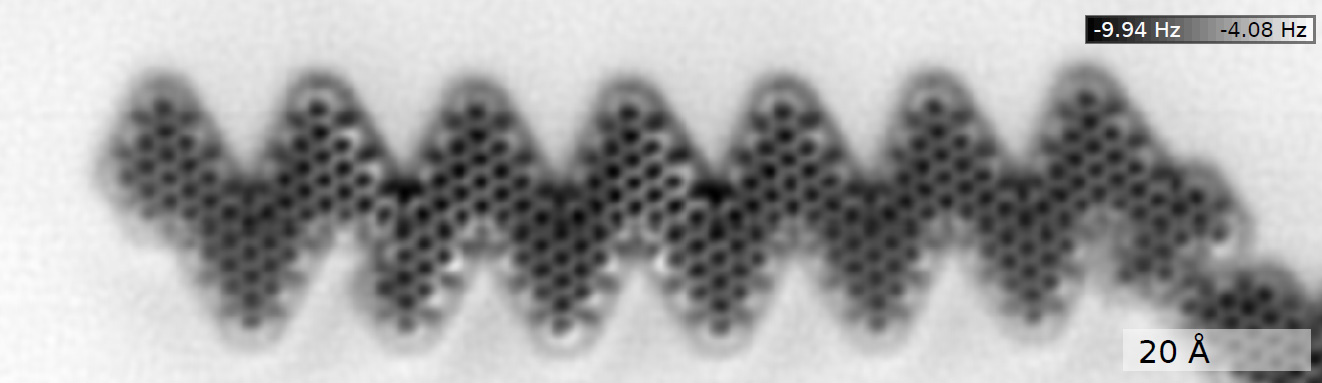 Sample NC-AFM data (frequency shift) of
custom designed precursors molecules which were
surface synthesized into GNR assemblies.
Data acquired using GXSM-3.0 + SR-MK3-A810/PLL
operating a modified CREATEC based LT-STM/AFM in
force detection mode, constant height operation at
approx. 70pm oscillation amplitude using a Q-Plus
(TM Franz J. Giessibl) Sensor @29.84kHz and a
"magic" functionalized tip not to be disclosed here.
Sample NC-AFM data (frequency shift) of
custom designed precursors molecules which were
surface synthesized into GNR assemblies.
Data acquired using GXSM-3.0 + SR-MK3-A810/PLL
operating a modified CREATEC based LT-STM/AFM in
force detection mode, constant height operation at
approx. 70pm oscillation amplitude using a Q-Plus
(TM Franz J. Giessibl) Sensor @29.84kHz and a
"magic" functionalized tip not to be disclosed here.
(*) NC-AFM detection is using a qPlus Sensor (TM) FJ. Giessibl at 30kHz. Frequency shift detection, constant height force (Freq. shift) mapping.
Scanning probe and optical microscopes for operation in air and controlled ambient
Contact: Xiao Tong
Park NX-20 atomic force microscope for surface imaging at ambient conditions at room temperature, as well as at elevated temperatures. It provides capabilities for standard contact and non-contact AFM operation, as well as Lateral Force Microscopy (LFM), Scanning Capacitance Microscopy (SCM), Magnetic Force Microscopy (MFM), Scanning Tunneling Microscopy (STM) and Nanolitography, among others.
WiTec Alpha combination microscope for atomic force microscopy, scanning near-field optical microscopy, confocal microscopy, and confocal Raman microscopy within the same field of view. Two laser excitation sources (633 nm and 532 nm) for confocal and confocal Raman microscopy. Operation between room temperature and 200°C.
Lab-based Ambient Pressure Photoelectron Spectroscopy (AP-PES)
Contact: J. Anibal Boscoboinik, Ashley Head
The lab-based AP-PES instrument allows for surface chemical analysis via core-level (XPS) and valance-level (UPS) photoelectron spectroscopy at gas pressures up to ~ 10 Torr and sample temperatures up to 500 °C. Applications include in-operando studies of surface chemistry, catalysis, and energy storage processes. This instrument is located at the CFN and has 4 photon sources: monochromated Al (1486.6 eV), Mg (1253.6 eV), Cr (5417 eV), and He (20.2, 40.8 eV). Differential pumping allows for gas pressures in the Torr range at the sample while maintaining ultrahigh vacuum conditions in the analyzer. Suitable sample types include single crystals, foils, and powders. Samples can be moved through the vacuum system to an infrared reflection absorption spectroscopy (IRRAS) chamber with a polarizer, where IR data can be collected under gas pressures ranging from UHV to ~20 Torr. Samples can be heated to 500 °C and cool to -180 °C. A sample preparation chamber connects the PES and IR chambers. Ar sputtering, cooling to -180 °C, heating to 900 °C, low gas dosing, and metal evaporation are available in the preparation chamber.
Ambient Pressure PES and IRRAS
This instrument allows for surface chemical analysis via X-ray Photoelectron Spectroscopy (XPS) and Infrared Reflection Absorption Spectroscopy (IRRAS) at gas pressures up to ~ 5 mbar and variable temperatures. Applications include in situ studies of surface chemistry, catalysis, separation, and energy storage processes, among others.
Low Energy Electron Microscope V (LEEM)
LEEM V:
A field-emission low-energy electron microscope (Elmitec LEEM V) allows for in-situ microscopic studies of dynamic surface processes.
Low-Temperature UHV Scanning Tunneling/Force Microscope
Createc LT-STM/AFM:
A upgraded Createc low-temperature UHV scanning tunneling microscope (STM) with atomic force microscope (NC-AFM/HR-AFM operation modes. Default operation at 5K STM and sample temperature. Using Q-Plus sensor (30kHz) with FIB shaped 25um PtIr tip wire. Full time support by CFN staff knowledgeable in various preparation methods for molecule structure imaging and beyond.
NanoIR/s-SNOM
NanoIR/s-SNOM:
The NanoIR instrument is capable of performing both scattering-type scanning near-field optical microscopy (s-SNOM) and photothermal infrared spectromicroscopy (PTIR) with a spatial resolution of 10nm in tapping mode and 50nm in contact mode.
Scanning Electron Microscope/Scanning Auger Microscopy/4-point Transport Measurement of Nanostructures
Nanoprobe:
This Nanoprobe system is capable of performing scanning electron microscopy (SEM), scanning Auger microscopy (nanoSAM), 4-point probe measurements, and low energy electron diffraction (LEED).
UHV Multiprobe Surface Analysis System - STM/XPS/UPS/ISS/LEED/TPD
Multiprobe
UHV-MultiProbe Surface Analysis System (STM\XPS\UPS\ISS\LEED\TPD) is capable of in-situ clean sample preparations, nanostructure fabrications, and complementary surface characterizations including atomic-resolution surface structures, chemical compositions/states, relative atomic concentrations, and physical and chemical properties, aimed at exploring structure-properties relationships.
mIRage O-PTIR + Raman
The mIRage optical-photothermal infrared (O-PTIR) plus Raman instrument provides sub-500nm spatially resolved infrared and Raman spectra on the same spot at the same time with the same spatial resolution.
Bruker Vertex 80v Spectrometer w/UHV IRRAS and Powder Transmission Capabilities
Bruker FTIR:
For transmission and reflectance IR measurements from UHV to atmospheric pressure.
Park NX-20 Atomic Force Microscope
AFM:
The Park NX-20 atomic force microscope is capable of surface imaging at ambient conditions at room temperature, as well as at elevated temperatures.
WiTec Alpha Combination Microscope
Raman:
WiTec Alpha 300 combination microscope integrates confocal Raman microscopy, atomic force microscope, scanning near-field optical microscope, confocal microscope within the same field of view.