Metasurfaces Shrink Broadband Photonics to Smallest Sizes Ever
July 19, 2017
What is the scientific achievement?
In analogy with Moore's Law for microelectronics, miniaturization of photonics increases the signal processing power of photonic integrated circuits. In this work, scientists have demonstrated the smallest and most broadband photonic integrated devices to date, by incorporating optical metasurfaces into the structure to control light propagation in waveguides.
Why does this achievement matter?
These small-footprint, broadband, and low-loss devices are highly desirable for photonic integrated circuits. The size reduction realized here is similar to that achieved in the 1950s when semiconductor transistors replaced vacuum tubes.
What are the details?
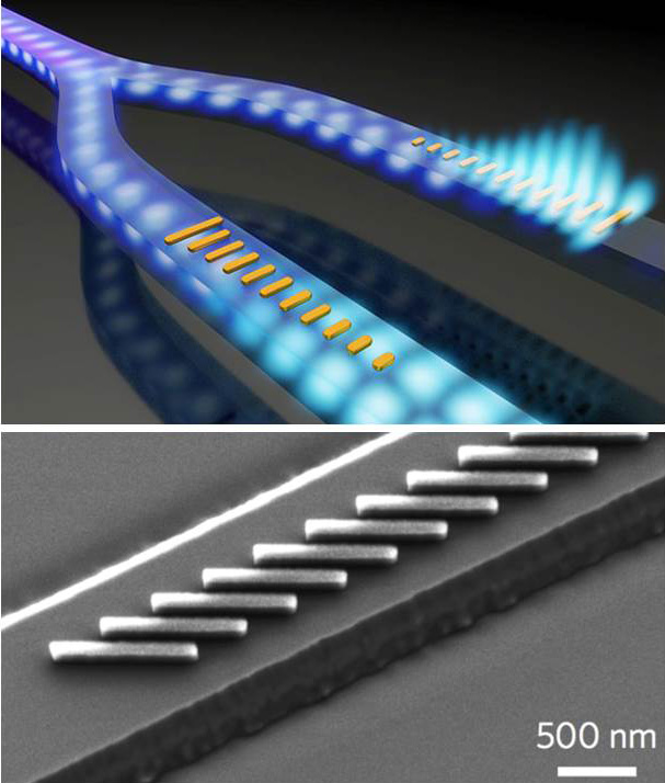 enlarge
(Top) Schematic of nanostructured metasurface atop an optical waveguide. (Bottom) Scanning electron microscope image of a fabricated gold matasurface patterned atop a lithium niobate waveguide.
CFN Capabilities:
Integrated photonic waveguide/metasurface devices were made using the CFN Nanofabrication Facility.
Publication Reference
Zhaoyi Li1, Myoung-Hwan Kim1,2, Cheng Wang3, Zhaohong Han, Sajan Shrestha, Adam Christopher Overvig, Ming Lu, Aaron Stein, Anuradha Murthy Agarwal, Marko Loncar, and Nanfang Yu, Controlling Propagation and Coupling of Waveguide Modes Using Phase-Gradient Metasurfaces, Nature Nanotechnology (2017) doi:10.1038/nnano.2017.50.
Collaborating Institutions:
1Department of Applied Physics and Applied Mathematics, Columbia University, New York, NY 10027, USA
2Department of Physics, The University of Texas Rio Grande Valley, Brownsville, TX 78520, USA
3John A. Paulson School of Engineering and Applied Sciences, Harvard University, Cambridge, Massachusetts 02138, USA
4Microphotonics Center and Department of Materials Science and Engineering, Massachusetts Institute of Technology, Cambridge, Massachusetts 02139, USA
5Center for Functional Nanomaterials, Brookhaven National Laboratory, Upton, NY 11973, USA
IEEE Spectrum: "Integrated Photonic Circuits Shrunk Down to the Smallest Dimensions Yet"
Science Daily: "Method to control light propagation in waveguides invented"
Phys.org: "Engineers invent method to control light propagation in waveguides"
Novus Light: "Optical Nano-Antennas Control Light Propagation in Waveguides"
Laser Focus World: "Waveguide mode converters have wide bandwidth, small footprint"
Acknowledgement of Support
The work was supported by the Air Force Office of Scientific Research (grant No. FA9550-14-1-0389 through a Multidisciplinary University Research Initiative program), Defense Advanced Research Projects Agency Young Faculty Award (grant No. D15AP00111), and National Science Foundation (grant No. ECCS-1307948). Funding from the Ministry of Defense, Singapore, and from the Defense Threat Reduction Agency Grant No. HDTRA1-13-1-0001 is gratefully acknowledged. A.C.O acknowledges support from the NSF IGERT program (grant No. DGE-1069240). Research was carried out in part at the Center for Functional Nanomaterials, Brookhaven National Laboratory, which is supported by the U.S. Department of Energy, Office of Basic Energy Sciences, under contract no. DE-SC0012704.
2017-12373 | INT/EXT | Newsroom