Innovative Photoresist Chemistry Brings Angstrom-Scale Patterning Within Reach
January 21, 2025
 enlarge
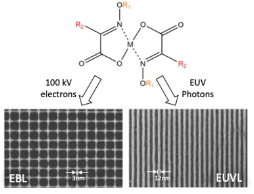
High atom-economy resist platform achieves uniform isolated 3 nm lines using EBL (left) and dense 12 nm lines using EUVL with line-width roughness < 2 nm (right)
Scientific Achievement
Researchers from Paul Scherrer Institute (Switzerland), CFN (USA), NUS and IMRE (Singapore) pioneered low-molecular weight photoresist platform enabling ultra high-resolution electron beam lithography (EBL) and extreme ultraviolet lithography (EUVL) with record low roughness.
Significance and Impact
This work tackles a key bottleneck in high-throughput, reliable EUV patterning of sub-10 nm device features, which is critical for high-volume manufacturing of cutting-edge computer chips and opens up pathway for achieving Angstrom resolution in lithography.
Research Details
Traditional organic, polymeric photoresists don’t meet the stringent requirements of chip manufacturing at Angstrom nodes and novel inorganic containing hybrid resist are necessary moving forward. In this collaborative work between PSI, CFN, NUS and IMRE, photoresist formulation is fundamentally reimagined as being made out of bare essential components — a metal atom efficient at absorbing EUV light and initiator that drives the intramolecular rearrangement leading to solubility change in the exposed resist. By changing the Metal core and organic ligands, many different combination of resist can be prepared – just like LEGO bricks.
The resists under this platform are amenable to patterning using both EBL, which is primarily used in research, and EUVL, which is only viable driver for industrial high-throughput sub-10 nm patterning. A record 1.9-2 nm isolated line features were patterned using EBL — best reported using any commercial EBL system and limited by the instrumental capability. 12 nm half-pitch line-space features were patterned using EUV interference lithography, all the while achieving record-low line-width roughness below 2 nm. There is room for improvement and resolve patterns smaller than 10 nm using EUVL. It is expected that the resist could enable even smaller pattern dimensions leading into the angstrom-scale.
- Resist assembled out of bare essentials – high EUV absorption metal and a radical initiator – flexibility of independently optimizing both
- High atom economy rendering ultrahigh resolution & ultralow roughness
Publication Reference
M. S. M. Saifullah,* A. K. Rajak, K. A. Hofhius, N. Tiwale, Z. Mahfoud, A. Testino, P. Karadan, M. Vockenhuber, V. A. Guzenko, D. Kazazis, S. Valiyaveettil, Y. Ekinci,* “Approaching Angstrom-Scale Resolution in Lithography Using Low-Molecular-Mass Resists (<500 Da),” ACS Nano 18, 24076 (2024)
DOI: https://doi.org/10.1021/acsnano.4c03939
OSTI: https://www.osti.gov/biblio/2448263
Acknowledgment of Support
This PSI led collaborative work used resources of the Nanofabrication facility of the Center for Functional Nanomaterials, which is a US Department of Energy Office of Science User Facility, at the Brookhaven National Laboratory under contract DE-SC0012704.
2025-22303 | INT/EXT | Newsroom