Advanced Electron Microscopy Reveals Processing Impacts on Quantum Circuits
April 21, 2025
 enlarge
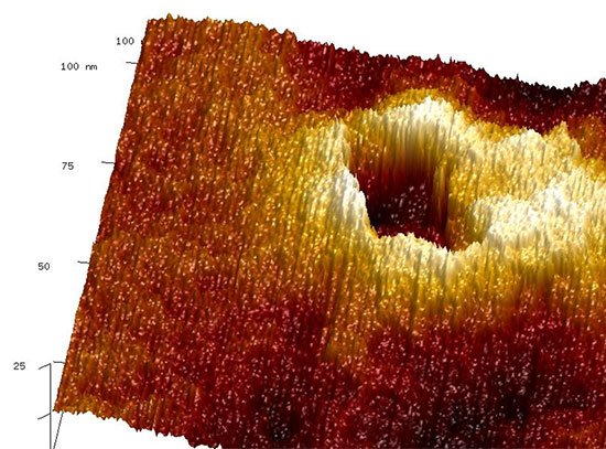
Transmission electron microscopy (TEM) imaging reveals processing-induced lattice strain and surface/bulk damage in superconducting resonators.
Scientific Achievement
Researchers from the Co-design Center for Quantum Advantage (C2QA) investigated how wet and dry etching processes affect the morphology, chemistry, and strain in high-Q tantalum resonators, currently the most promising materials for high-performance superconducting qubits.
Significance and Impact
Processing-induced effects, such as lattice deformations and substrate damage, can influence the performance of superconducting quantum devices. Understanding these effects and their impact helps optimize device fabrication.
Research Details
Superconducting resonators play a pivotal role in various quantum technology applications, such as quantum computing and high-frequency communication systems. The performance of these resonators is closely tied to the properties of the superconducting films used in their fabrication. In this study, C2QA researchers used resources at the Center for Functional Nanomaterials to investigate the impact of wet and dry etching on tantalum (Ta) films, leveraging advanced scanning transmission electron microscopy-based characterization methods, and examined the morphological, chemical, and strain changes caused by the etching processes. Consequently, the group report the significant differences between the two etching methods, with dry etching resulting in straight slanted sidewalls and a thinner oxidized layer, while wet etching produced curved sidewalls and undercuts. Both methods led to the formation of a residual Ta wedge at the lower part of the sidewall, causing lattice deformation, which could adversely influence the homogeneous operations of superconducting devices. These insights enhance our understanding of how etching influences superconducting films, offering valuable guidance for optimizing resonators and related devices. These findings mark a significant stride in advancing quantum technologies and high-frequency communication by enhancing our practical understanding of superconducting material fabrication.
- Advanced scanning transmission electron microscopy reveals that both dry etching and wet etching introduce lattice strain and processing damage to resonators.
- Dry etching produces thinner sidewall oxide layers than wet etching but creates more substrate damage.
Publication Reference
J. Mun, C. Zhou, K. Kisslinger, M. Liu*, and Y. Zhu*, “Comparative S/TEM study of superconducting Ta quantum resonators by wet and dry etching types”, Appl. Phys. Lett. 125, 164002 (2024).
DOI: https://doi.org/10.1063/5.0233167
OSTI: https://www.osti.gov/biblio/2478779
Acknowledgment of Support
This work is supported primarily by the U.S. Department of Energy (DOE), Office of Science, National Quantum Information Science Research Centers, Co-design Center for Quantum Advantage (C2QA) under Grant No. DE-SC0012704. Transmission Electron Microscopy work at Brookhaven National Laboratory (BNL) was supported by DOE/BES, Department of Materials Science and Engineering. This research used Electron Microscopy resources of the Center for Functional Nanomaterials (CFN), which is a U.S. DOE Office of Science User Facility, at BNL. All the above BNL facilities are under Grant No. DE-SC0012704. The authors thank Dr. Nana Shumiya and Prof. Nathalie P. de Leon at Princeton University for providing their Ta superconducting resonators and their helpful descriptions of fabrication methods.
2025-22489 | INT/EXT | Newsroom