Solving the Riddle of the Crystal Structure of Borophene
January 22, 2019
What is the scientific achievement?
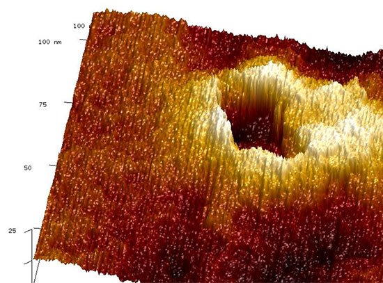
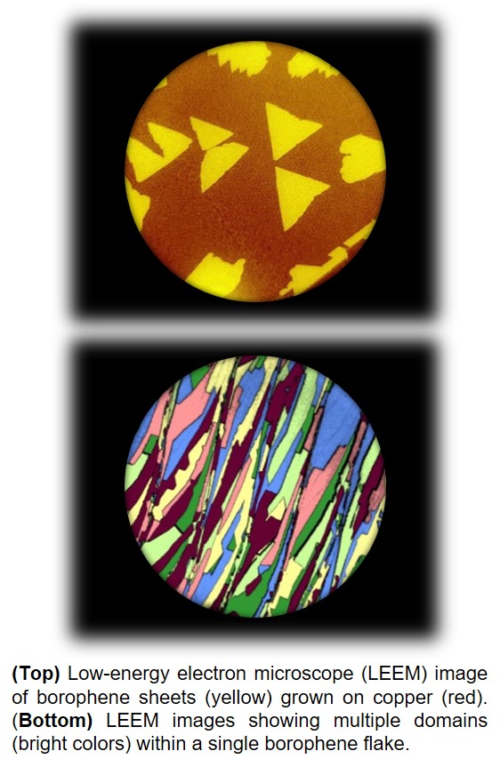
CFN users from Yale University and BNL have developed a new synthesis method for borophene — single-atom sheets of boron — a material predicted to have remarkable electronic properties. The new synthesis approach facilitates growth of the largest single crystal domains of borophene produced to date (100 μm2) — large enough to definitively measure the crystal structure and resolve a debate in the scientific community.
Why does this achievement matter?
Borophene is a 2D electronic material with promise for next-generation electronic devices, including quantum information science. The improved growth method makes possible future fabrication of the first borophene electronic devices.
What are the details?
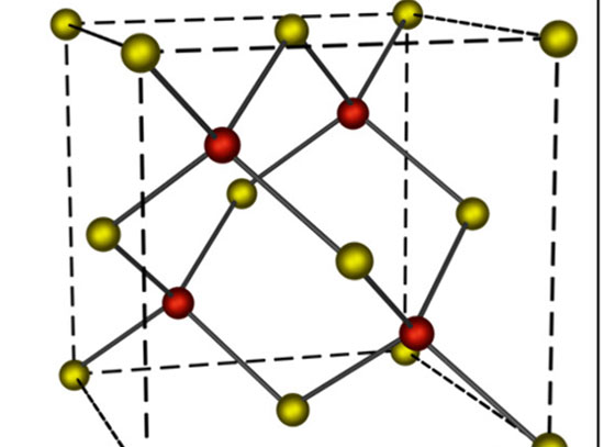
Borophene is a two-dimensional (2D) boron allotrope that has attracted much attention as a candidate material platform for high-speed, transparent, and flexible electronics. The material has been previously synthesized on silver (111) substrates and studied by tunneling and electron spectroscopy. However, borophene’s exact crystal structure remains controversial because the nanometer-size single-crystal domains produced to date prohibit detailed studies. In this work, CFN users from Yale University and BNL report a new synthesis of borophene monitored in-situ by low-energy electron microscopy, diffraction, and scanning tunneling microscopy (STM), and modelled by ab initio theory. The study resolves the crystal structure and phase diagram of borophene grown on Ag(111), but find that the domains remain nanoscale for all growth conditions. However, borophene grown on Cu(111) by this method produces single-crystal domains as large as 100 μm2 in area. The borophene crystal structure is resolved as a triangular network having a concentration of hexagonal vacancies of η = 1/5. Our experimental data, together with first principles calculations, indicate charge-transfer coupling to the substrate without significant covalent bonding. This work sets the stage for fabricating borophene-based electronic devices.
CFN Capabilities:
The CFN low-temperature scanning tunneling microscope/atomic force microscope was used for borophene characterization and imaging.
Publication Reference
R. Wu, I. K. Drozdov, S. Eltinge, P. Zahl, S. Ismail-Beigi, I. Božovic, A. Gozar, Large-area single-crystal sheets of borophene on Cu(111) surfaces, Nature Nanotechnology 14, 44 (2018).
DOI: 10.1038/s41565-018-0317-6
https://phys.org/news/2018-12-borophene-advances-d-materials-platform.html
https://www.sciencedaily.com/releases/2018/12/181203131102.htm
https://news.yale.edu/2018/12/03/yale-scientists-make-borophene-breakthrough
https://www.bnl.gov/newsroom/news.php?a=113226
Acknowledgement of Support
This research was supported by the US Department of Energy, Basic Energy Sciences, Materials Sciences and Engineering Division. R.W. and A.G. are supported by the Gordon and Betty Moore Foundation’s EPiQS Initiative through grant GBMF4410. I.K.D. acknowledges the support of a BNL Gertrude and Maurice Goldhaber Distinguished Fellowship. This research used resources of the Center for Functional Nanomaterials, which is a US DOE Office of Science Facility, at Brookhaven National Laboratory under contract no. DE-SC0012704. S.E. is supported by the National Science Foundation Graduate Research Fellowship through grant DGE-1122492. S.E and S.I.-B. thank the computing resources provided by the staff of the Yale University Faculty of Arts and Sciences High Performance Computing Center as well as NSF XSEDE resources via grant TG-MCA08X007.
2019-14348 | INT/EXT | Newsroom