Nanocrystals Within Nanowires
January 22, 2016
What Is The Scientific Achievement?
 enlarge
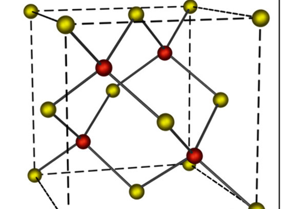
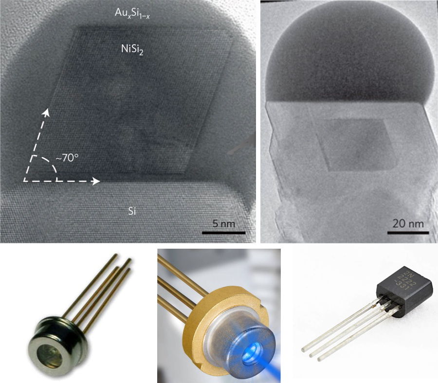
Top: High-resolution electron microscopy images of a nickel silicide rhombic nanocrystal embedded in a silicon nanowire prepared with gold silicide used as a catalyst. The images demonstrate the intimate interactions that arise at the interfaces of these nanomaterials. Bottom: The physical properties that arise from such complex nanosystems could be used in next-generation photodetectors, lasers, and transistors.
Semiconducting nanowires have a wide range of existing and potential applications in optoelectronic materials, from single-electron transistors and tunnel diodes, to light-emitting semiconducting nanowires to energy-harvesting devices. An international collaboration led by the University of Cambridge and IBM, has demonstrated a new method to create novel nanowires that contain nanocrystals that are embedded within them. This accomplished by modifying the classic “vapor-liquid-solid” crystal growth method, wherein a liquid phase catalyst is used to both decompose an incoming gas-phase source and mediate the deposition of the solid, growing nanowire. In this work, a bimetallic catalyst is used, and it was shown that by appropriate thermal treatment that it is possible to crystallize a solid silicide structure within the liquid catalyst, and then attach the nanowire to the solid silicon in a controlled epitaxial fashion. This leads to exquisite control over these structures at the nanoscale, and opens up a wide range of potential device structures.
Why Does This Matter?
This development could lead to new classes of nanoscale devices, with a range of potential applications from single-electron transistors and tunnel diodes to photodetectors and semiconductor lasers.
What Are The Details?
CFN Capabilities: CFN’s Electron Microscopy Facility was used to image the complex nanomaterials by high spatial-resolution, aberration-corrected transmission electron microscopy. A first-of-its-kind direct electron detector was used to obtain high temporal-resolution images of the fabrication process.
Publication Reference
Synthesis of nanostructures in nanowires using sequential catalyst reactions
F. Panciera,1,2 Y.-C. Chou,2,3,4 M.C. Reuter,2 D. Zakharov,4 E.A. Stach,4 S. Hofmann1 and F.M. Ross2
1 Department of Engineering, Cambridge University, Cambridge, UK, CB3 0FA
2 IBM Research Division, T. J. Watson Research Center, Yorktown Heights, NY 10598
3 Department of Electrophysics, National Chiao Tung University, Hsinchu City, Taiwan
4 Center for Functional Nanomaterials, Brookhaven National Laboratory, Upton, New York 11973
Nature Materials 14, 820 (2015)
Acknowledgement of Support:
Supported by the National Science Foundation under Grants No. DMR-0606395 and 0907483 (Y.-C.C.), ERC Grant 279342: InSituNANO (F.P. and S.H.), the National Science Council of Taiwan under Grant No. NSC-101-2112-M-009-021-MY3 (Y.-C.C.), the Center for Interdisciplinary Science under the MOE-ATU project for NCTU (Y.-C.C.). Research performed in part at the Center for Functional Nanomaterials, Brookhaven National Laboratory, which is supported by the US Department of Energy, Office of Basic Energy Sciences, under contract DE-AC02-98CH10886 (D.Z. and E.A.S.).
2016-6201 | INT/EXT | Newsroom