Positioning Nitrogen-Vacancy Centers for Diamond-Based Quantum Computers
June 1, 2016
What Is The Scientific Achievement?
Realizing a solid-state quantum computer would usher in a new era of computing due to this architecture's ability to perform certain types of calculations significantly faster than computing schemes used today. One promising pathway to produce solid-state quantum computers involves using the quantized spins of nitrogen-vacancy (NV) centers in diamond to process quantum information. Properly positioning these centers into arrangements that are suitable for quantum computation is a substantial challenge. This work implemented a nanofabrication-based solution that patterned chains of NV centers with higher spatial resolution and placement accuracy than any previous effort. These diamond-based NV centers stand as feasible, functioning building blocks for quantum computer components.
Why Does This Matter?
The silicon-based stencils, fabricated at CFN and used to pattern the NV centers, possessed features as small as two nanometers—nearly 10× smaller than any previous demonstration. This represents a wholly suitable pathway for the production of quantum logic gates, a critical component for quantum computing architectures.
What Are The Details?
Among the hundreds of color centers in diamond, only a few defects are known to have electron spin states that can be initialized and measured optically. These include as yet unidentified centers and silicon vacancies as well as the nitrogen vacancy (NV) center, which to date has been studied most extensively. The NV electron spin triplet levels can be manipulated by microwave pulses and exhibit coherence times exceeding milliseconds at room temperature and approaching one second at liquid nitrogen temperature. These exceptional properties have enabled demonstrations of qubit gates, quantum registers, and NV−photon and NV−NV entanglement. <
 enlarge
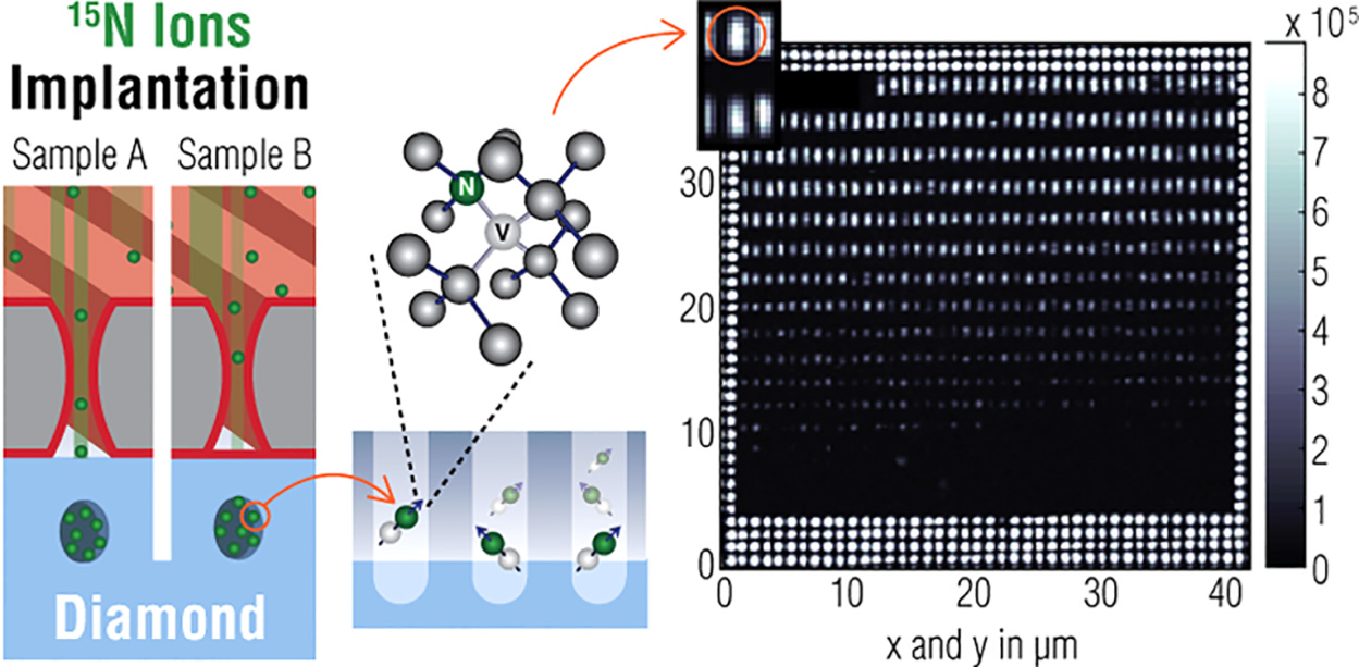
Left: Graphic demonstrating the process of implanting nitrogen ions through apertures for creating NV-s. Right: Confocal image scan of an array of NV- spin chains. Each line (circled in red) represents an individual chain.
Here, we present an implantation technique based on masks produced from 270 nm thick silicon-on-oxide (SOI) membranes by a combination of EBL lithography and atomic layer deposition (ALD), enabling arbitrarily narrow (measured here below 1 nm) implantation lines with high aspect ratio. This approach combines the low FWHM of the AFM tip implantation with the high throughput of EBL patterning while achieving the excellent aspect ratio of randomly patterned implantation masks (mica). We employ these masks to fabricate rectangular NV implantation regions in which the smaller dimension has a FWHM as low as 1 nm, reaching a regime where the N distribution is no longer limited by the feature size of the mask but by the fundamental process of implanted nitrogen scattering in the diamond lattice. This approach opens the door to scalable fabrication of isolated spin ensembles for quantum information processing and quantum transport measurements.
CFN Capabilities: NV stencils were fabricated by reactive ion etching and electron-beam lithography in the CFNs Nanofabrication Facility and by atomic layer deposition in CFN’s Material Synthesis Facility. Transmission and scanning electron microscopy were performed in CFN’s Electron Microscopy Facility.
Publication Reference
Generation of Ensembles of Individually Resolvable Nitrogen Vacancies Using Nanometer-Scale Apertures in Ultrahigh-Aspect Ratio Planar Implantation Masks
Igal Bayn,†,‡,? Edward H. Chen,†,? Matthew E. Trusheim,†,? Luozhou Li,† Tim Schröder,† Ophir Gaathon,†,‡ Ming Lu,§ Aaron Stein,§ Mingzhao Liu,§ Kim Kisslinger,§ Hannah Clevenson,† and Dirk Englund†
† Department of Electrical Engineering and Computer Science, and Research Lab of Electronics, Massachusetts Institute of Technology, 77 Massachusetts Avenue, Building 36-575, Cambridge, Massachusetts 02139, United States
‡ Department of Electrical Engineering, Columbia University, New York, New York 10027, United States
§ Center for Functional Nanomaterials, Brookhaven National Laboratory, Upton, New York 11973, United States
Nano Letters 15, 1751 (2015)
Acknowledgement of Support:
Financial support was provided in part by the W.M. Keck Foundation, GTech MURI, and AFOSR PECASE. E.H.C. and H.C. were supported by the NASA Office of the Chief Technologist’s Space Technology Research Fellowship. M.T. was funded by the NSF IGERT program Interdisciplinary Quantum Information Science and Engineering. T.S. acknowledges support by the Alexander von Humboldt foundation. The authors would like to thank Alexey Tkachenko for insightful discussions and Xinwen Yao and Nathalie de Leon for help in diamond preparation. This research was carried out in part at the Center for Functional Nanomaterials, Brookhaven National Laboratory, which is supported by the U.S. Department of Energy, Office of Basic Energy Sciences, under Contract No. DE-AC02-98CH10886.
2016-6628 | INT/EXT | Newsroom