Nanodiamonds Shine with Single Photons
January 31, 2020
What is the scientific achievement?
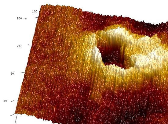
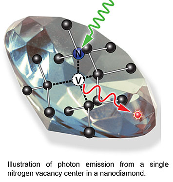
Scientists from MIT and CFN researchers have developed a new, scalable approach to creating highly-uniform single-crystal nanodiamonds. The team combined self-assembled nanopatterning with plasma etching for precise synthesis of large quantities of 30 nm diameter nanodiamonds. Photoluminescence measurements demonstrated single-photon emission from single nitrogen vacancy centers located within the nanodiamonds.
Why does this achievement matter?
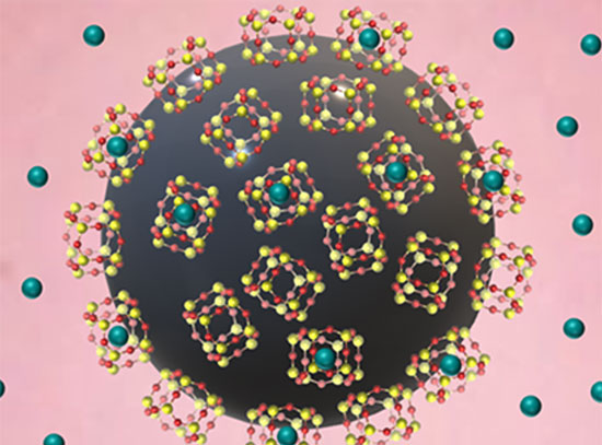
Solid-state defects are a leading material system candidate for quantum communication and sensing. Single optical defects in nanodiamonds have potential as a sensor platform with unparalleled sensitivity.
What are the details?
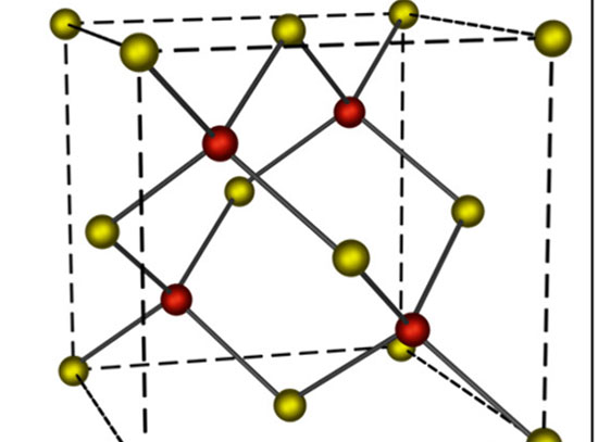
The diamond nitrogen vacancy (NV) center, with its optically-addressable long-lived spin system, is well suited for applications ranging from quantum networks to quantum sensors. Nanodiamonds (ND) hosting such color centers are promising for various biological and quantum technologies, thanks in part to their compatibility with biologically active tissue and with common surface modification techniques. A reliable fabrication method of non-aggregated, uniform-sized, monocrystalline NDs with incorporated single color centers is still challenging. In this work, the authors developed a technique that allows large-scale parallel fabrication of non-aggregated, uniform-sized, monocrystalline NDs hosting single NV centers. The fabrication technique starts with CVD grown high-purity single-crystal diamond. It leverages the scalability of block copolymer (BCP) self-assembly combined with sequential infiltration synthesis to define nanometer-sized etching masks across an arbitrarily large diamond sample. A directional plasma etching step defines the dimensions of the NDs. An isotropic plasma etching step releases the NDs. Single-photon emission from single NVs hosted in the fabricated NDs was confirmed using photoluminescence measurements. Statistics of the diameter of the released NDs indicate a mean diameter of about 30 nm with a variance of 5.4 nm.
CFN Capabilities
CFN Materials Synthesis and Nanofabrication Facilities were used for nanodiamond fabrication. The Advanced Optical Spectroscopy & Microscopy Facility was used for photoluminescence measurements.
Publication Reference
J. Zheng, B. Lienhard, G. Doerk, M. Cotlet, E. Bersin, H.S. Kim, Y.C. Byun, C.Y. Nam, J. Kim, C.T. Black, D. Englund, Top-down fabrication of high-uniformity nanodiamonds by self-assembled block copolymer masks, Scientific Reports 9, 6914 (2019).
DOI: https://doi.org/10.1038/s41598-019-43304-5
Acknowledgement of Support
The conducted research was supported in part by the Army Research office MURI biological transduction program and NSF Center for Integrated Quantum Materials. Research carried out in part at the Center for Functional Nanomaterials, Brookhaven National Laboratory, which is supported by the U.S. Department of Energy, Office of Basic Energy Sciences, under Contract No. DE-SC0012704. J.Z. was supported in part by Master Dynamic, Inc.
2020-17090 | INT/EXT | Newsroom


