Atomic-Resolution Imaging of Bulk Samples by Scanning Electron Microscopy
July 23, 2024
 enlarge
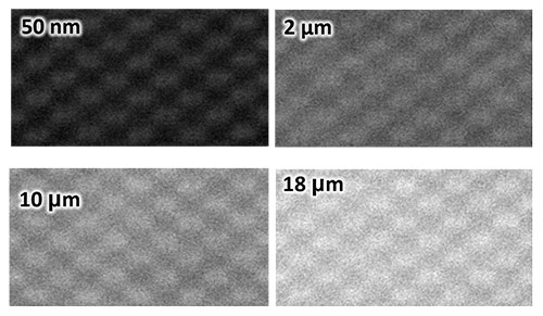
Atomically-resolved secondary electron images of crystalline silicon, acquired from different sample thicknesses
Scientific Achievement
Center for Functional Nanomaterials and Brookhaven National Laboratory researchers demonstrated atomic-resolution secondary electron imaging in bulk crystalline samples as thick as 18 µm, using an aberration-corrected scanning transmission electron microscope.
Significance and Impact
This breakthrough enables high-resolution atomic-scale imaging of bulk materials without the need for ultra-thin specimens, which are typically required for electron microscopy at this resolution.
Research Details
Transmission electron microscopy (TEM) has been instrumental in providing atomic-scale resolution insights into materials. However, its efficacy hinges on thin specimens for electron transparency, necessitating a meticulous sample thinning process. This research showcases the viability of attaining atomic-level details from thick, bulk samples, which better reflect the properties of real materials. Leveraging an aberration-corrected scanning transmission electron microscope (STEM) with a secondary electron (SE) detector, the team captured images of bulk specimens. A silicon specimen, shaped like an isosceles right-angle triangle with sides measuring 18 µm, was meticulously prepared using a focused ion beam. (The geometry allowed for the determination of sample thickness, particularly useful for thicker specimens). The team observed that the atomic structure persists throughout the entire thickness range (up to 18 µm) of the SE images. Although there is a gradual increase in background intensity with thickness, the intensity remains consistent at atomic positions in silicon, which suggests a limited contribution from SEs generated by backscattered electrons, a conclusion supported by multi-slice calculations. The calculations also indicate that the quality of SE images should remain reasonably high for bulk samples exceeding 50 μm in thickness. This study illustrates the feasibility of attaining atomic resolution in SE images of bulk samples using 200 kV electrons. This breakthrough opens up new avenues for investigating the atomic-scale structure of materials without requiring thin samples.
- Multi-slice calculations confirm atomic resolution is due to limited contributions from backscattered electrons & focusing of secondary electrons
- These calculations suggest feasibility of atomic scale imaging in samples as thick as 50 µm.
Publication Reference
S. Hwang, L. Wu, K. Kisslinger, J. Yang, R. Egerton, Y. Zhu, “Secondary-electron imaging of bulk crystalline specimens in an aberration corrected STEM”, Ultramicroscopy, 261, 113967 (2024).
DOI: https://doi.org/10.1016/j.ultramic.2024.113967
OSTI: https://www.osti.gov/biblio/2338119
Acknowledgment of Support
We appreciate Dr. Xiao Tong for the discussion about AFM results. This research was supported by supported by Department of Energy, Basic Energy Science, Materials Science & Engineering Division, and it used the Electron Microscopy Facility of the Center for Functional Nanomaterials (CFN), which is a U.S. Department of Energy Office of Science User Facility at Brookhaven National Lab (Contract No. DE-SC0012704). RFE thanks the Natural Sciences and Engineering Research Council of Canada for a Discovery Grant.
2024-22057 | INT/EXT | Newsroom


