Metal-Semiconductor-Metal Ion-Implanted Si Waveguide Photodetectors
July 8, 2014
 enlarge
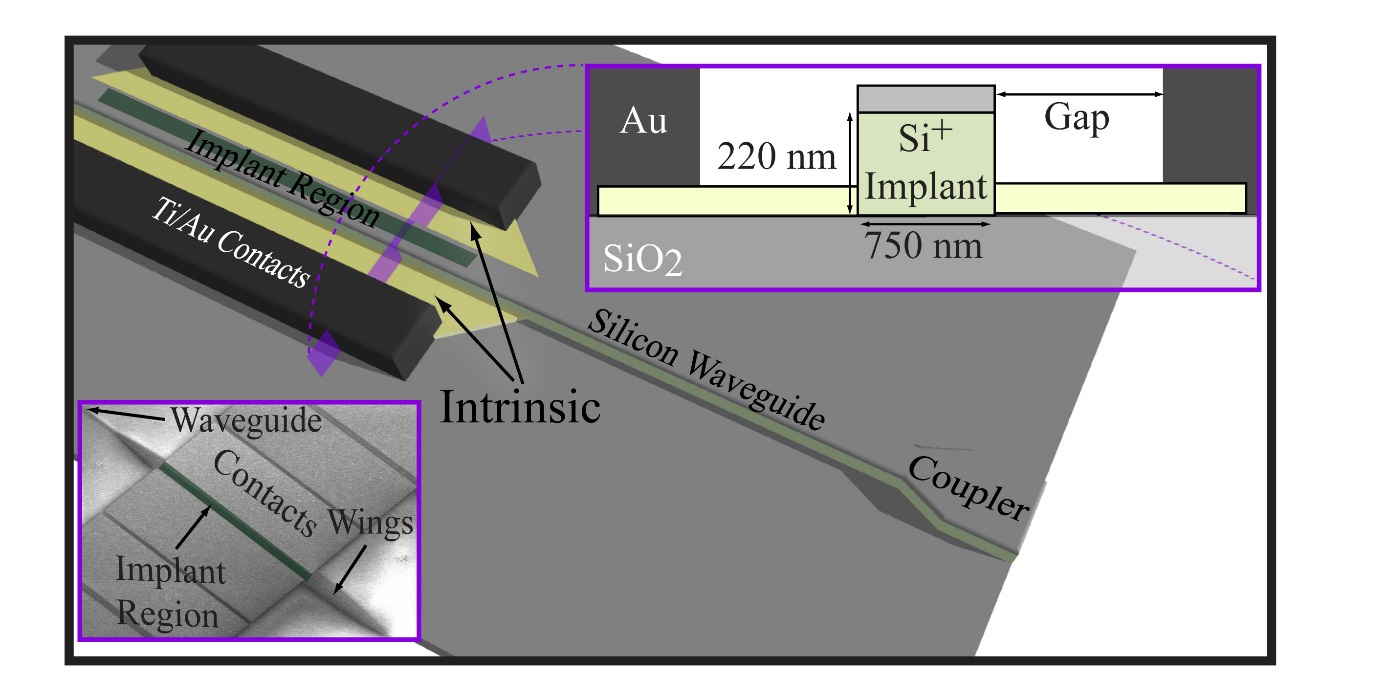
Figure 1: Device cartoon highlighting structure with the bottom inset showing SEM top view of the device and the top inset showing the cross-section of the MSM structure.
What Is The Scientific Achievement?
A new integrated Metal-Semiconductor-Metal (MSM) waveguide structure for silicon-based nanowire waveguide photodetectors has been demonstrated with responsivities of greater than 0.5 A/W at a wavelength of 1550 nm for a device length of 1mm. Sub-bandgap absorption in the silicon waveguide was achieved by creating divacancy lattice defects via silicon ion implantation. The modal absorption coefficient of the ion-implanted silicon waveguide was measured to be ≈ 185 dB/cm, resulting in a detector responsivity of ≈ 0.51 A/W at a 50V bias. The frequency response of a typical 1mm-length detector was measured to be 2.6 GHz, with simulations showing that a frequency response of 9.8 GHz was achievable with an optimized contact configuration and bias voltage of 15V. Due to the ease with which these devices can be fabricated, and their potential for high performance, these detectors are suitable for various applications in silicon -based photonic integrated circuits.
Why Does This Matter?
The majority of ion-implanted silicon waveguide photodetectors devices are based on reverse biased p-i-n rib waveguide diodes. These p-i-n diodes require multiple masking and alignment steps, and have significant junction capacitance. The lower capacitance/length makes the MSM ideally suited for the longer low-absorption-coefficient ion-implanted silicon waveguide PDs. Additionally, the lack of contact doping makes the MSM useful for carrier removal in nonlinear four-wave mixing devices.
What Are The Details?
- CFN Capabilities: The Nanofabrication Facility’s JEOL 6300 e-beam lithography tool and Oxford Plasmalab Reactive Ion Etcher were crucial in fabricating the silicon nanowire waveguides, providing a mean sidewall roughness on the order of 3nm, resulting in minimal waveguide scattering loss.
- The reduced junction capacitance of an MSM allows for longer NWWG PDs suitable for the lower absorption coefficients associated with these ion-implanted detectors without sacrificing frequency response. These devices are also used to study new ion-implanted mid-IR Si-NWWG PDs and can be incorporated with our Si-nanowire photonic crystals for resonant cavity enhanced absorption.
Publication Reference
Metal-semiconductor-metal ion-implanted Si waveguide photodetectors for C-band operation
Brian Souhan1, Richard R. Grote1, Jeffrey B. Driscoll1, Ming Lu2, Aaron Stein2, Hassaram Bakhru3, and Richard M. Osgood, Jr.1
1Microelectronics Sciences Laboratories, Columbia University, New York, New York 10027, USA
2Center for Functional Nanomaterials, Brookhaven National Laboratory, PO Box 5000, Upton, New York 11973, USA
3College of Nanoscale Science and Engineering, State University of New York at Albany, Albany, New York 12222, USA
Optics Express 22, 9150-9158 (2014).
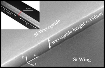
Figure 2: SEM view of Si waveguide sidewalls shows < 3 nm roughness. Inset: Si photonic crystal resonant enhanced absorber.
Acknowledgment of Support
Research carried out in part at the Center for Functional Nanomaterials, Brookhaven National Laboratory, which is supported by the U.S. Department of Energy, Office of Basic Energy Sciences, under Contract No. DE-AC02-98CH10886. The authors also acknowledge support from the Columbia Optics and Quantum Electronics IGERT under NSF grant DGE-1069420.
2014-5037 | INT/EXT | Newsroom