Tracking Electrons on the Move in Twisted Graphene
September 30, 2021
 enlarge
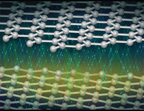
Artistic representation of an electron beam interacting with a 30-degree-twisted bilayer of graphene. The impinging electron wave interacts with graphene, undergoing resonances, which can be detected by analyzing the electron wave reflected back.
What is the scientific achievement?
CFN scientists studying two different configurations of bilayer graphene—the two-dimensional, atomically thin form of carbon—detected interlayer electronic resonances, in which electrons bounce between the atomic planes at the interface. Using the electronic signatures of these states, the scientists found that twisting one graphene layer by 30 degrees relative to the other shifts the resonance, consistent with an increased distance between layers in the twisted configuration.
Why does this achievement matter?
Interlayer interactions change with the interlayer distance, influencing how electrons move. An understanding of this motion could inform the design of quantum technologies for more powerful computing and more secure communication.
What are the details?
Today’s computer chips are based on our knowledge of how electrons move in semiconductors, specifically silicon, but the physical properties of silicon are reaching a physical limit in terms of how small transistors can be made and how many can fit on a chip. If we can understand how electrons move at the small scale of a few nanometers in the reduced dimensions of 2-D materials, we may be able to unlock another way to utilize electrons for quantum information science.
In this study, the team used a simple material model—bilayer graphene in stacked and twisted configurations—to investigate quantum confinement effects. To probe the interlayer interactions, they injected an electron beam into the material with a low-energy electron microscope (LEEM) and detected the reflected electrons. This LEEM is part of the x-ray photoemission electron microscopy (XPEEM)/LEEM endstation of the Electron Spectro-Microscopy beamline (21-ID) at the NSLS-II; the CFN operates this endstation through a partner user agreement with NSLS-II. The scientists also shot photons from a laser-based optical microscope with a spectrometer into the material and analyzed the spectrum of light scattered back. This microscope is part of the Quantum Material Press, an automated tool under development at the CFN for the synthesis, processing, and characterization of layered 2-D materials. The experimental results revealed that that twisting one of the graphene layers by 30 degrees relative to the other increases the distance between the two layers by about six percent relative to the non-twisted configuration, influencing how electrons move in the bilayer system. Theoretical calculations verified the unique resonant electronic behavior of the twisted configuration. An understanding of this electron motion could inform the design of future quantum technologies for more powerful computing and more secure communication.
CFN Capabilities
The CFN Quantum Material Press and the CFN XPEEM/LEEM endstation, operated in partnership with NSLS-II at the ESM beamline, were used to characterize the optical and electronic properties of bilayer graphene.
Publication Reference
Z. Dai, Z. Gao, S.S. Pershoguba, N. Tiwale, A. Subramanian, Q. Zhang, C. Eads, S.A. Tenney, R.M. Osgood Jr., C.-Y. Nam, J. Zang, A.T. Charlie Johnson, J.T. Sadowski. “Quantum-well bound states in graphene heterostructure interfaces,” Physical Review Letters 127, 086805 (2021).
DOI: https://doi.org/10.1103/PhysRevLett.127.086805
OSTI: https://www.osti.gov/biblio/1817199-quantum-well-bound-states-graphene-heterostructure-interfaces
Brookhaven Lab press release: “Layered Graphene with a Twist Displays Unique Quantum Confinement in 2-D”
PennToday news story: “Atomically-thin, twisted graphene has unique properties”
Brookhaven Lab feature story: “Building a Printing Press for New Quantum Materials”
Brookhaven Lab postdoc spotlight: “Zhongwei Dai: Exploring the Strange Quantum World of 2D Materials”
Acknowledgement of Support
This research used resources from the Center for Functional Nanomaterials and the National Synchrotron Light Source II, which are U.S. Department of Energy (DOE) Office of Science facilities at Brookhaven National Laboratory, under Contract No. DE-SC0012704. Z.G., Q.Z., and A.T.C.J. acknowledge support from the National Science Foundation through MRSEC DMR1720530 and EAGER 1838412. Z.G. acknowledges support from the Research Grant Council of Hong Kong SAR (Project No. 24201020) and a Direct Grant from The Chinese University of Hong Kong (Project No. 4055121). J.Z. and S.P. acknowledge financial support by the U.S. Department of Energy (DOE), Office of Science, Basic Energy Sciences (BES) under Award No. DE-SC0020221.
2021-19235 | INT/EXT | Newsroom


