Block Copolymer-Templated Dielectrics Alter Graphene Band Structure
July 22, 2025
 enlarge
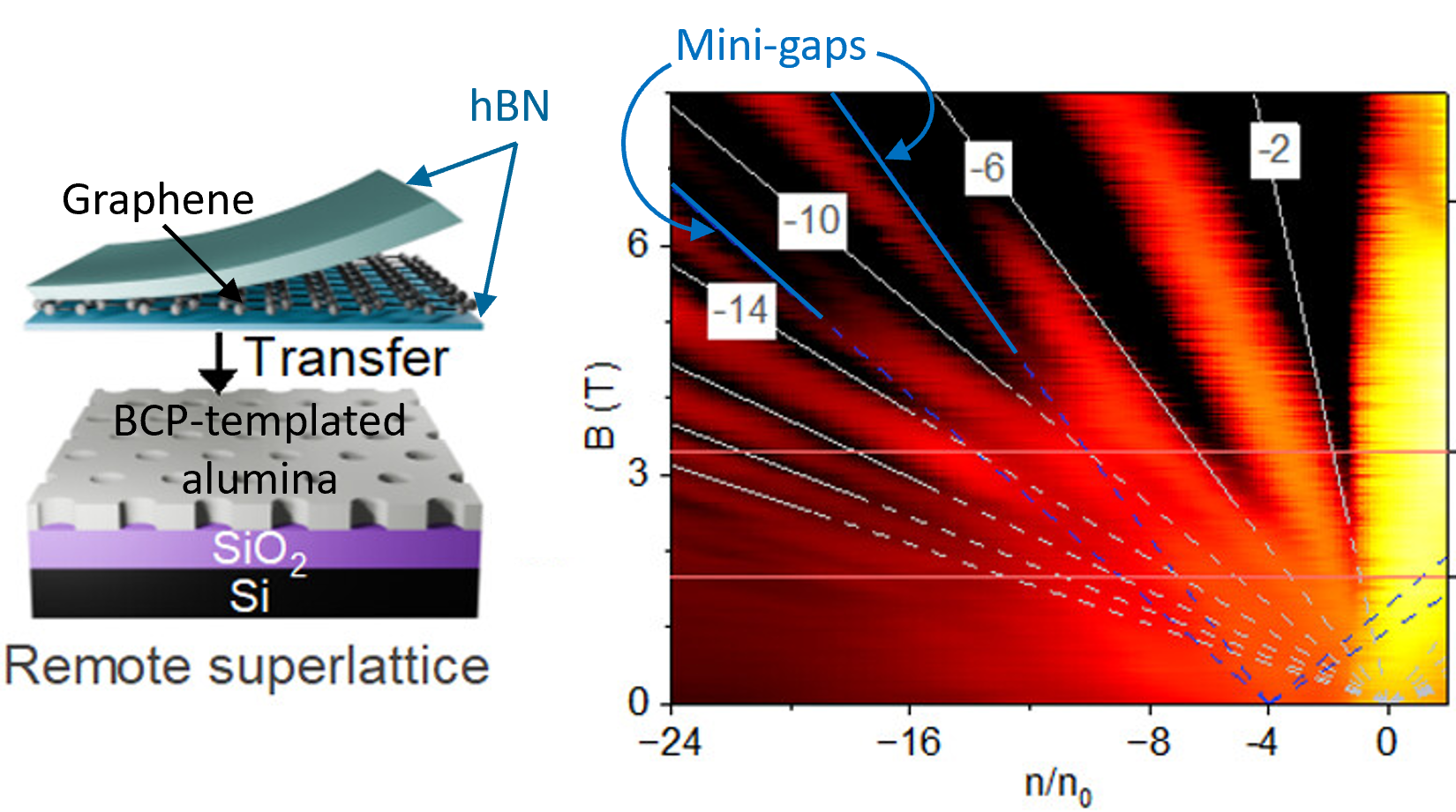
Block copolymer-templated, high dielectric constant films with periodic nanoholes form patterned superlattice potentials in overlying graphene (left) that induce formation of Hofstadter mini-gaps in the graphene band structure (right).
Scientific Achievement
NYU and CFN researchers demonstrated an “etch-free” approach using block copolymer (BCP)-templated “high-k” dielectric nanopatterns to create periodic electrostatic superlattice (SL) potentials in graphene, altering its band structure.
Significance and Impact
This scalable, cost-effective approach to SL engineering opens new pathways for modifying the electronic behavior of 2D materials – crucial for developing next-generation quantum and nanoscale electronic devices.
Research Details
Introducing nanoscale periodic superlattice potentials into 2D van der Waals materials like graphene is a powerful way to engineer their electronic band structures and introduce intriguing quantum properties. Conventionally, these potentials are achieved by twisting 2D material multilayers to create Moiré potentials, or by nanopatterning and etching a gate electrode or dielectric in proximity to the graphene. Both approaches face significant challenges in terms of fabrication complexity, cost, and resilience. Researchers from New York University (NYU) and the Center for Functional Nanomaterials (CFN) developed a simple and scalable alternative approach to fabricate artificial superlattices exploiting the self-assembly of block copolymer thin films. Through vapor phase infiltration of alumina selectively into one polymer block, nanopatterned gate dielectrics with tunable capacitance can be formed without any direct etching of the dielectric. Upon applying a voltage, these nanopatterned gate dielectrics induce periodic superlattice potentials in the graphene, as evidenced in electronic transport measurements by the presence of replica Dirac points and Hofstadter mini-gaps. Surprisingly, these potentials are observed despite the presence of rotational disorder that is intrinsic to self-assembled nanopatterns. This work outlines a strategy for cost-effective fabrication of artificial dielectric superlattices with engineered symmetries, periodicities and dielectric strengths for rationally engineering 2D material electronic band structures.
- “High-k” aluminum oxide dielectric nanopatterns (38 nm period) were fabricated using self-assembled BCP films via vapor phase infiltration.
- Despite the rotational disorder, graphene transport measurements showed clear replica Dirac points and Hofstadter mini-gaps, both hallmarks of periodic SL potentials, induced by the nanopatterns.
- The method introduces an approach to generating SL potentials over large areas without 2D material twisting or nanopattern etching.
Publication Reference
M. Jamalzadeh, Z. Zhang, Z. Huang, M. Manzo-Perez, K. Kisslinger, T. Taniguchi, K. Watanabe, P. Moon, G.S. Doerk*, D. Shahrjerdi*, “Synthetic Band Structure Engineering of Graphene Using Block Copolymer-Templated Dielectric Superlattices”, ACS Nano 19, 9885 (2025).
DOI: https://doi.org/10.1021/acsnano.4c14500
Acknowledgment of Support
The authors acknowledge support from NSF, award # 2224139, and NYU Nanofabrication facility for device fabrication. This research used the Materials Synthesis and Characterization and Electron Microscopy facilities of the Center for Functional Nanomaterials (CFN), which is a U.S. Department of Energy Office of Science User Facility, at Brookhaven National Laboratory under Contract No. DE-SC0012704.
2025-22676 | INT/EXT | Newsroom