Resisting Moore's Law Limits with Hybrid Materials
November 30, 2021
 enlarge
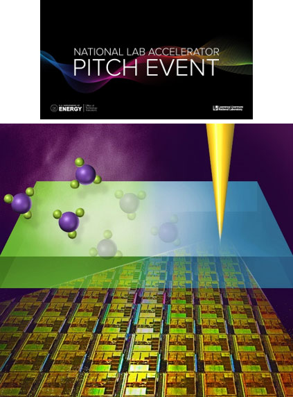
Inorganic elements (red) are infused into an existing organic photoresist (blue) on a silicon wafer (gray) through vapor processing. The resulting organic-inorganic hybrid photoresist (purple) can be exposed to extreme-ultraviolet light to manufacture extremely downscaled next-generation semiconductor devices.
What is the scientific achievement?
A CFN-led team developed new hybrid resists for transferring circuit patterns onto semiconductor substrates by infusing vapors of inorganic elements into organic resists. With a model system (aluminum-oxide-infiltrated PMMA), they demonstrated easy control of resist composition and performance characteristics like sensitivity, contrast, and etch resistance. For example, the silicon etch selectivity can be 300x higher than that for proprietary resists.
Why does this achievement matter?
Resists with high sensitivity and etch resistance are needed for high-volume semiconductor manufacturing via extreme-ultraviolet lithography. This advanced patterning technique promises to extend Moore’s law, reducing feature sizes to one nanometer for smaller, faster, and more energy-efficient electronics.
What are the details?
Miniaturizing semiconductor devices is becoming ever more critical to extend Moore’s law and increase the energy efficiency and performance of future computing hardware. Extreme-ultraviolet (EUV) lithography is the only technology that can support not only the current state-of-the-art semiconductor manufacturing but also continued semiconductor device downscaling to one nanometer. However, EUV lithography suffers from reduced manufacturing productivity compared with previous-generation patterning technologies. This reduced productivity is primarily due to the low EUV sensitivity of conventional organic photoresists—the radiation-sensitive materials applied to semiconductor substrates to create nanoscale patterns. Hybrid photoresists containing both organic and inorganic materials are emerging as a solution because of the high EUV sensitivity of inorganic elements. However, chemical synthesis of hybrid photoresists is complex, rendering timely optimization of photoresist composition and performance (as per manufacturing requirements) highly challenging.
Here, we demonstrate a new type of hybrid photoresists based on vapor-phase infiltration of inorganic elements into existing organic photoresists. Our method enables facile control of hybrid resist composition and performance parameters—including sensitivity, contrast, and etch resistance—without complex chemical synthesis. For proof of concept, we synthesized hybrid organic-inorganic resists containing poly(methyl methacrylate), or PMMA, and aluminum oxide. By exploiting the enhanced etch selectivity of these hybrid resists, exceeding that of costly proprietary resists and a “hard” mask layer such as silicon dioxide, we patterned high-resolution, high-aspect-ratio silicon nanostructures through electron-beam lithography. This technology has the potential to produce new hybrid EUV photoresists that combine high EUV sensitivity and etch resistance for next-generation semiconductor manufacturing by EUV lithography.
CFN Capabilities
The resists were fabricated and characterized in the CFN Materials Synthesis and Characterization and Electron Microscopy Facilities.
Publication Reference
N. Tiwale, A. Subramanian, K. Kisslinger, M. Lu, J. Kim, A. Stein, and C.-Y. Nam, “Advancing next generation nanolithography with infiltration synthesis of hybrid nanocomposite resists,” Journal of Materials Chemistry C 7, 29 (2019).
DOI: https://doi.org/10.1039/C9TC02974E
OSTI: https://www.osti.gov/pages/biblio/1561253
Brookhaven Lab news release: "Next-Gen Semiconductor Manufacturing Tech Wins DOE National Pitch Competition"
Brookhaven Lab feature story: "Synthesis Method Expands Material Possibilities"
Brookhaven Lab news release: "Enhancing Materials for Hi-Res Patterning to Advance Microelectronics”
Acknowledgment of Support
The authors thank Dr. Xiao Tong for his assistance with AFM measurements and Dr. Dmytro Nykypanchuk for ellipsometry measurements. The research was carried out at the Center for Functional Nanomaterials (CFN), Brookhaven National Laboratory (BNL), which is supported by the U.S. Department of Energy, Office of Basic Energy Sciences, under Contract No. DE-SC0012704.
2021-19373 | INT/EXT | Newsroom