Watching Gallium Nitride Nanowires Grow at the Atomic Scale
May 1, 2016
What Is The Scientific Achievement?
Nitride materials have had a considerable impact on the technology landscape, with light emitting diodes (LEDs) rapidly displacing conventional light bulbs and providing advances in solid state electronics. Despite these existing commercial applications, further technological developments could be realized if higher quality nitride crystals—particularly gallium nitride (GaN)—can be grown without defects.
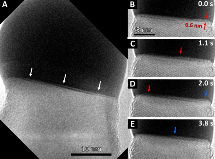
One favorable option to produce high quality, commercially viable GaN crystals is to grow them as nanowires. In this work, environmental transmission electron microscopy (ETEM) was used to image the crystal growth process of these nanowires both in real time and at the atomic scale. The study discovered that the wire grows by multiple double-bilayer atomic steps, which is contrary to the conventional wisdom since most nanowires grow in a single bilayer layer-by-layer fashion.
Why Does This Matter?
 enlarge
Images from an ETEM video of a GaN wire growing within an ammonia and trimethylgallium environment at 800 °C. Multiple atomic steps are observed at the interface of the growth catalyst and the nanowire, indicated by arrows.
 enlarge
Gallium nitride materials have enabled common technologies, such as blue LEDs, green lasers and LED-based light bulbs, leading to significant energy savings worldwide.
What Are The Details?
Nitride materials have had a considerable impact on the technology landscape, with LEDs rapidly displacing conventional light bulbs and providing advances in solid state radar electronics. Despite these existing commercial applications, further technological improvements could be enabled if higher quality nitride crystals could be grown. Nitrides—in particular GaN—are notoriously difficult to grow without defects, especially on low cost substrates such as silicon.
A nanowire provides a structure that could produce crystals of exceptional quality on cheaper substrates. However, little is understood about the atomistic details of GaN growth. Here, environmental transmission electron microscopy (ETEM) was used to image the crystal growth process in real time, and at the atomic scale. It was found that the wire grows by multiple double-bilayer atomic steps: this is highly unusual as most nanowires grow in a single bilayer layer-by-layer fashion.
CFN Capabilities: CFN’s Electron Microscopy Facility was used for atomic-scale imaging of the nanowire crystal growth.
Publication Reference
Atomic Resolution in-situ Imaging of a Double-Bilayer Multistep Growth Mode in Gallium Nitride Nanowires
Andrew D. Gamalski†, Jerry Tersoff‡, and Eric A. Stach†
† Center for Functional Nanomaterials, Brookhaven National Laboratory, Upton, New York 11973
‡ IBM Research Division, T. J. Watson Research Center, Yorktown Heights, New York 10598
Nano Letters 16, 2283 (2016)
Acknowledgement of Support:
Research supported at the Center for Functional Nanomaterials, which is a U.S. DOE Office of Science Facility, at Brookhaven National Laboratory under Contract No. DESC0012704. We gratefully acknowledge the use of facilities within the LeRoy Eyring Center for Solid State Science at Arizona State University. We acknowledge assistance from Karl Weiss at Arizona State University. We acknowledge Gwen Wright for providing assistance with sample preparation. Helpful discussions with Frances Ross and Federico Panciera are gratefully acknowledged.
2016-6625 | INT/EXT | Newsroom