Bi-functional Nanocrystal Coatings Enhance the Performance of Silicon Solar Cells
June 30, 2016
What Is The Scientific Achievement?
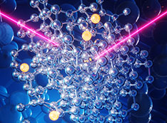
New mechanisms are continuously being sought to improve the performance of solar cell devices. A promising approach exploits energy transfer processes within novel architectures that combine layers of nanocrystals with materials that possess high charge mobility, like silicon. To date, fundamental questions persist regarding how different energy transfer processes quantitatively contribute to solar cell performance. A collaboration among CFN and Stony Brook University have implemented this energy transfer mechanism in model hybrid solar cells, comprised of ultrathin silicon and layers of nanocrystals. The bi-functionality of the nanocrystal layers within the hybrid architecture enhanced the overall power conversion efficiency by up to 45%: ~40% arose from efficient energy transfer between the nanocrystals and the silicon, and ~5% came from the nanocrystal film’s antireflective effects..
Why Does This Matter?
These studies showed the performance benefits of sensitizing silicon solar cells with nanocrystal layers and provide guidelines for designing enhanced light harvesting capabilities into otherwise conventional devices.
What Are The Details?
 enlarge
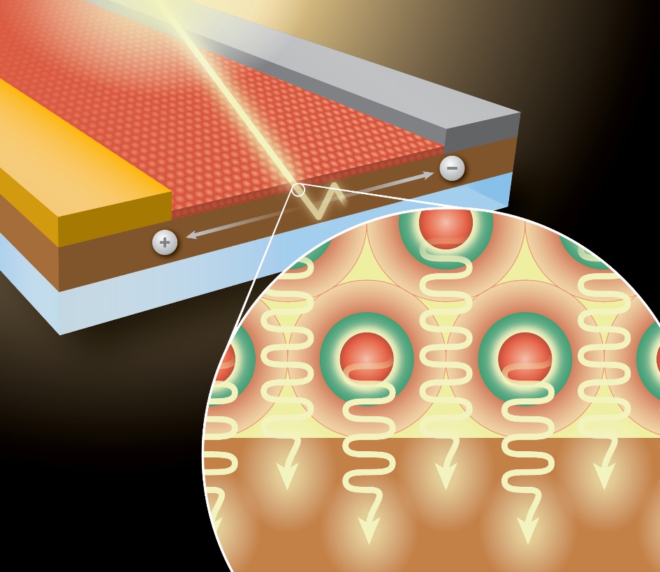
This study represents the first experimental implementation of a new solar cell architecture, which exploits energy transfer from nanocrystals to ultrathin silicon. The scheme described in this work improved the power conversion efficiency of base ultrathin Si solar cells via two distinctive routes, one emerging from the energy transfer and the other from the classical anti-reflective effects of nanocrystal layers. The realized solar cell performance enhancement and quantitative mechanistic understanding provides a pathway for the rational application of energy transfer schemes in solar panels.
In this work, we report the ET-driven enhancement of PV performance in an ultrathin Si solar cell architecture consisting of semiconductor NC energy donor layers atop an ultrathin Si energy acceptor with an incorporated in-plane Schottky junction. The well-defined layered device geometry not only decouples the NC energy donor layer from the charge transport and extraction processes in the Si solar cell but also enables us to combine the complementary investigative methods, including PV device characterization, time-resolved optical spectroscopy, transfer-matrix optical simulation, and dipole radiation theory calculation. By using this approach, we establish a quantitative mechanistic understanding of how different ET modes, distinguished from the intrinsic optical interference effects, contribute to the light harvesting in the functioning inorganic solar cells and clearly demonstrate the positive contribution of ET to the enhancement of the device PCE, primarily driven by the effective long-range radiative ET that improves the solar spectrum absorption in the ultrathin Si active layer.
CFN Capabilities: CFN’s Nanofabrication Facility was used to fabricate the solar cells and to characterize the hybrid cell architecture. CFN’s Advanced Optical Spectroscopy and Microscopy Facility was used to assess the cells’ light harvesting capabilities via transient absorption spectroscopy.
Publication Reference
Enhanced photovoltaic performance of ultrathin Si solar cells via semiconductor nanocrystal sensitization: energy transfer vs. optical coupling effects
Son Hoanga, Ahsan Ashrafbc, Matthew D. Eisamanbcd, Dmytro Nykypanchuka and Chang-Yong Nama
a Center for Functional Nanomaterials, Brookhaven National Laboratory, Upton, New York 11973, USA.
b Sustainable Energy Technologies Department, Brookhaven National Laboratory, Upton, New York 11973, USA
c Department of Physics and Astronomy, Stony Brook University, Stony Brook, New York 11794, USA
d Department of Electrical and Computer Engineering, Stony Brook University, Stony Brook, New York 11794, USA
Nanoscale 8, 5873 (2016)
Acknowledgement of Support:
This research was carried out at the Center for Functional Nanomaterials (S. H., D. N., C.-Y. N.) and Sustainable Energy Technologies Department (A. A. and M. D. E.), and Brookhaven National Laboratory (BNL), which is supported by the U.S. Department of Energy, Office of Basic Energy Sciences, under Contract no. DE-SC0012704.
2016-6629 | INT/EXT | Newsroom