- Home
- Facilities
- Research
-
Working at CFN
- Arrival & Departure
- Reports & Publications
- Acknowledging Use of CFN Facilities
- Data Management
- The Guide to Brookhaven
Safety Procedures
- Operations Plan
- Experimental Safety Reviews (ESR)
- COSA Training
- Hours of Operation
- Laser System Qualification
- Transport of Hazardous Materials
- Vendor On-site Scheduling Procedure (PDF)
- Electrical Equipment Inspections
- News & Events
- People
- Jobs
- Contact
- Business
- Intranet
Research Highlights

Arbitrary Design of DNA-Programmable 3D Crystals through Symmetry Mapping
CFN researchers and collaborators developed a symmetry-mapping algorithm, MOSES, that streamlines the design of DNA voxels and can be generalized to patchy particles.
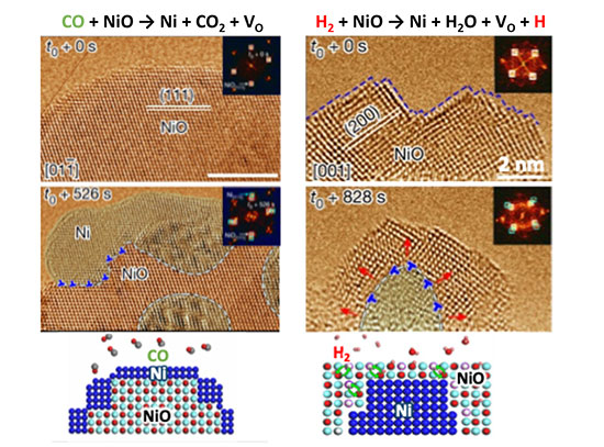
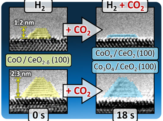
Gas-Dependent Oxide Reduction Revealed at the Atomic Scale
By revealing gas-dependent reduction dynamics, this work provides a mechanistic foundation for metal production and catalyst design.
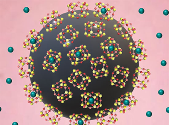
Simple Method for Trapping of Xenon in Nanocages
Researchers demonstrated a scalable and cost-effective method for trapping Xe, a scarce noble gas relevant to nuclear energy, nuclear safety, non-proliferation, medical imaging, and space propulsion.
Insights into EUV Resist Molecular Uniformity through Nano-Projectile SIMS
This capability provides a powerful new method for understanding and optimizing hybrid resists—key materials for advancing extreme ultraviolet (EUV) lithography in next-generation semiconductor manufacturing.
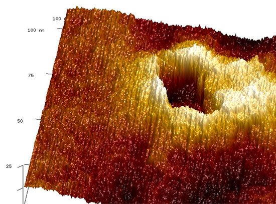
Reactant-Gas-Induced Nanoparticle Dynamics Depend on Size
We observe size-dependent morphological dynamics of supported metal nanoparticles (NPs) induced by interaction with reactant gases and find these are correlated with reaction pathway and product selectivity.

VISION: Voice-Controlled AI for Next-Gen Scientific Experimentation
This advance showcases how AI can seamlessly extend human interaction with complex scientific instruments, laying foundational infrastructure for AI-augmented scientific discovery.
Block Copolymer-Templated Dielectrics Alter Graphene Band Structure
NYU and CFN researchers demomonstrated a cost-effective approach to superlattice engineering opens new pathways for modifying the electronic behavior of 2D materials – crucial for developing next-generation quantum and nanoscale electronic devices.

Scalable Device Fabrication using DNA Self-Assembly
CFN led a project that created a scalable nanofabrication technique that integrates DNA-based self-assembly with conventional top-down approaches to create a 3D nanostructured device with photocurrent response.

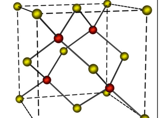
Octo-diamond Crystal of Nanoscale Tetrahedra Unlock Interchanging Chirality
Researchers from CFN, University of Michigan, and Columbia University discovered a new low-density "octo-diamond" crystal structure assembled from nanoscale tetrahedra (TH) of gold, featuring chiral bilayers that give rise to surface chiroptical properties.
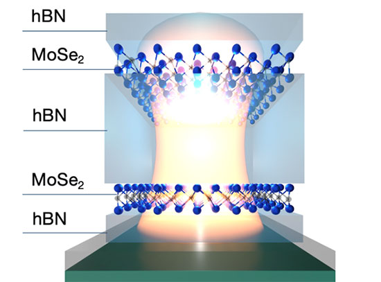
Atomically Thin Mirrors: A New Frontier in Light Confinement
This work establishes a new platform for nanoscale light manipulation using atomically thin materials, with potential use in quantum information processing, optical computing, and quantum photonics.
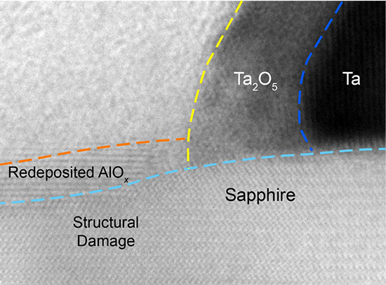
Advanced Electron Microscopy Reveals Processing Impacts on Quantum Circuits
Understanding these effects and their impact helps optimize quantum device fabrication.
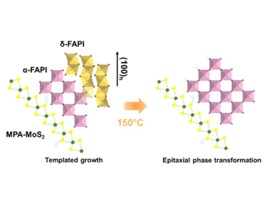
2D MoS2 Templates Unlock High-Performance Perovskite Solar Cells
The work reveals a new mechanism by which 2D additives control crystallization and boost hybrid perovskite performance for solar energy conversion and optoelectronics applications.